Shift register

a technology of shift register and shift register, which is applied in the field of shift register to achieve the effects of reducing the layout area increasing the driving capability of the output reset transistor, and reducing the reset time of the output signal

Inactive Publication Date: 2012-09-27
SHARP KK
View PDF3 Cites 26 Cited by
  • Summary
  • Abstract
  • Description
  • Claims
  • Application Information

AI Technical Summary

Benefits of technology

[0022]According to the first aspect of the present invention, if the clock signal is inputted when the output transistor is in the ON state, the potential of the control terminal of the output transistor becomes the post-boot potential that is higher than the ON potential (or lower than the ON potential) of the output transistor. Therefore, it is possible to increase the driving capability of the output reset transistor by connecting the control terminal of the output reset transistor to the control terminal of the output transistor included in the next stage unit circuit so as to apply the post-boot potential outputted from the next stage unit circuit to the control terminal of the output reset transistor. Accordingly, it is possible to reduce reset time of the output signal, or to reduce the layout area of the output reset transistor.
[0023]According to the second aspect of the present invention, by providing the state reset transistor, the output transistor can be controlled to be in the OFF state.
[0024]According to the third aspect of the pre...

Problems solved by technology

Further, as a method of downsizing display devices, there is known a method of monolithically providing a scanning signal line drive circu...

Method used


Image

  • Shift register
  • Shift register
  • Shift register

Examples


first embodiment

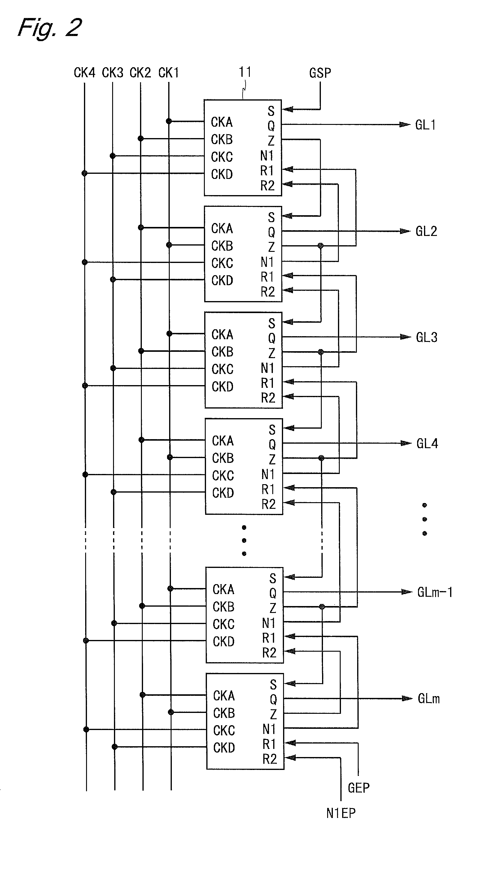
[0056]FIG. 2 is a block diagram showing a configuration of a shift register according to a first embodiment of the present invention. The shift register shown in FIG. 2 includes m unit circuits 11 arranged one-dimensionally. In the following description, a unit circuit 11 in an i-th position (i is an integer not smaller than 1 and not greater than m) is referred to as an i-th unit circuit UC (i). In this embodiment, m is assumed to be a multiple of 2.

[0057]The shift register shown in FIG. 2 is supplied with four clock signals CK1 to CK4 as the gate clock signal GCK, a single signal as the gate start pulse signal GSP, and a first gate end pulse signal GEP and a second gate end pulse signal N1EP as the gate end pulse signal GEP.

[0058]Each unit circuit 11 is supplied with the four clock signals CKA, CKB, CKC, and CKD, a set signal S, a state reset signal R1, an output reset signal R2, and a low level potential VSS (not shown). Each unit circuit 11 outputs an output signal Q, an additio...

second embodiment

[0099]FIG. 9 is a block diagram showing a configuration of a shift register according to a second embodiment of the present invention. FIG. 9 shows m unit circuits 11 arranged one-dimensionally. A first shift register is configured by cascade-connecting odd-numbered ones of the m unit circuits 11. Similarly, a second shift register is configured by cascade-connecting even-numbered ones of the m unit circuits 11. In the following, differences between this embodiment and the first embodiment will be described, and the features provided in common with the first embodiment will not be described. In this embodiment, m is assumed to be a multiple of 4.

[0100]The two shift registers shown in FIG. 9 are supplied with the four clock signals CK1 to CK4 as the gate clock signal GCK, a first gate start pulse signal GSP1 and the second gate start pulse signal GSP2 as the gate start pulse signal GSP, and a first gate end pulse signal GEP1, a second gate end pulse signal GSP2, a third gate end puls...


PUM


Abstract

Unit circuits 11 each including a TFT T2 (output transistor), a TFT T1 (input transistor), and a TFT T8 (output reset transistor) are cascade-connected, and a gate terminal of the TFT T8 is connected to a gate terminal of the TFT T2 included in a next stage unit circuit 11. By applying a post-boot potential that is higher than an ON potential of the TFT T8 to the gate terminal of the TFT T8, driving capability of the TFT T8 is increased. Accordingly, it is possible to reduce falling time duration of the output signal Q and a layout area of the TFT T8. In this manner, a shift register with a small area capable of resetting an output signal at high speed is provided.

Description

TECHNICAL FIELD[0001]The present invention relates to shift registers, and in particular to a shift register suitably used in a drive circuit for a display device, and the like.BACKGROUND ART[0002]An active matrix-type display device selects two-dimensionally arranged pixel circuits by line, and writes gradation voltages to the selected pixel circuits according to a video signal, thereby displaying an image. Such a display device is provided with a scanning signal line drive circuit including a shift register, in order to select the pixel circuits by line.[0003]Further, as a method of downsizing display devices, there is known a method of monolithically providing a scanning signal line drive circuit on a display panel along with pixel circuits using a manufacturing process of providing TFTs (Thin Film Transistors) within the pixel circuit. A display panel having a scanning signal line drive circuit monolithically provided is also referred to as a gate driver monolithic panel.[0004]A...

Claims


Application Information

Patent Timeline
IPC IPC(8): G09G5/00G11C19/00
CPCG09G3/3677G11C19/184G09G2310/0286G09G2300/0408G11C19/28
Inventor OHARA, MASANORI
Owner SHARP KK
Why Eureka
Try Eureka