Level shifter with balanced rise and fall times

a level shifter and shifter technology, applied in logic circuits, pulse automatic control, pulse techniques, etc., can solve the problems of difficult to achieve balanced delay times (rise and fall), delay can further vary, and the operation conditions and/or process variations are very difficult to achiev

Inactive Publication Date: 2010-10-05
AVAGO TECH INT SALES PTE LTD
View PDF9 Cites 29 Cited by
  • Summary
  • Abstract
  • Description
  • Claims
  • Application Information

AI Technical Summary

Problems solved by technology

For applications in which level shifters are included in timing signal paths, ensuring predictable signal delays can present design challenges.
While a conventional approach can attempt to tune the above delays (for example, by sizing transistors) to try to create equal values for Delay_HI and Delay_LO, such a balance is very difficult to achieve over wide range of operating conditions and / or process variations.
Further, these delays can further vary due to manufacturing process variations and / or operating temperature.
All of the above make it difficult to achieve balanced delay times (rise and fall) utilizing conventional techniques.

Method used


Image

  • Level shifter with balanced rise and fall times
  • Level shifter with balanced rise and fall times
  • Level shifter with balanced rise and fall times

Examples


Embodiment Construction

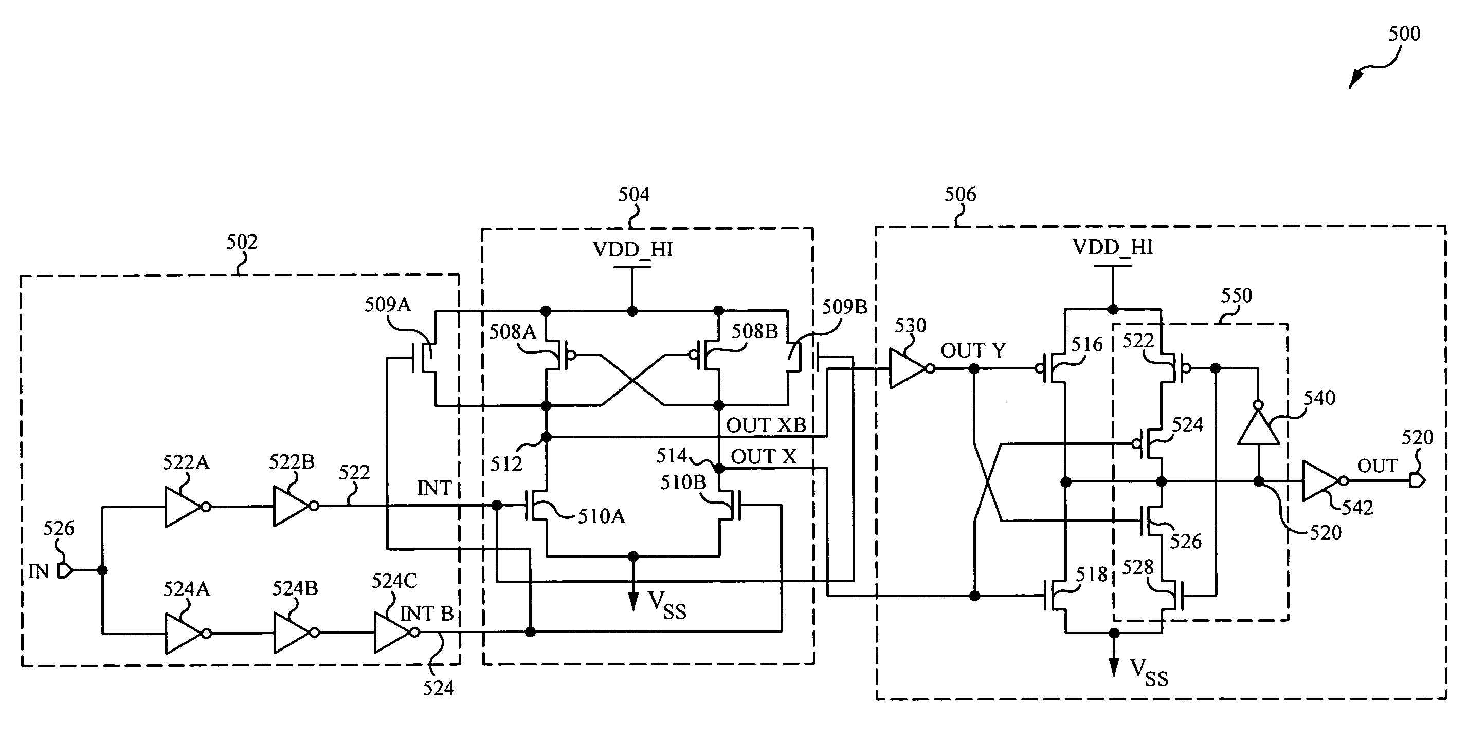
[0022]Various embodiments of the present invention will now be described in detail with reference to a number of drawings. The embodiments include level shifting circuits that can produce shifted signal levels with balanced rise and fall delays, and signal balancing methods for level shifting circuits.

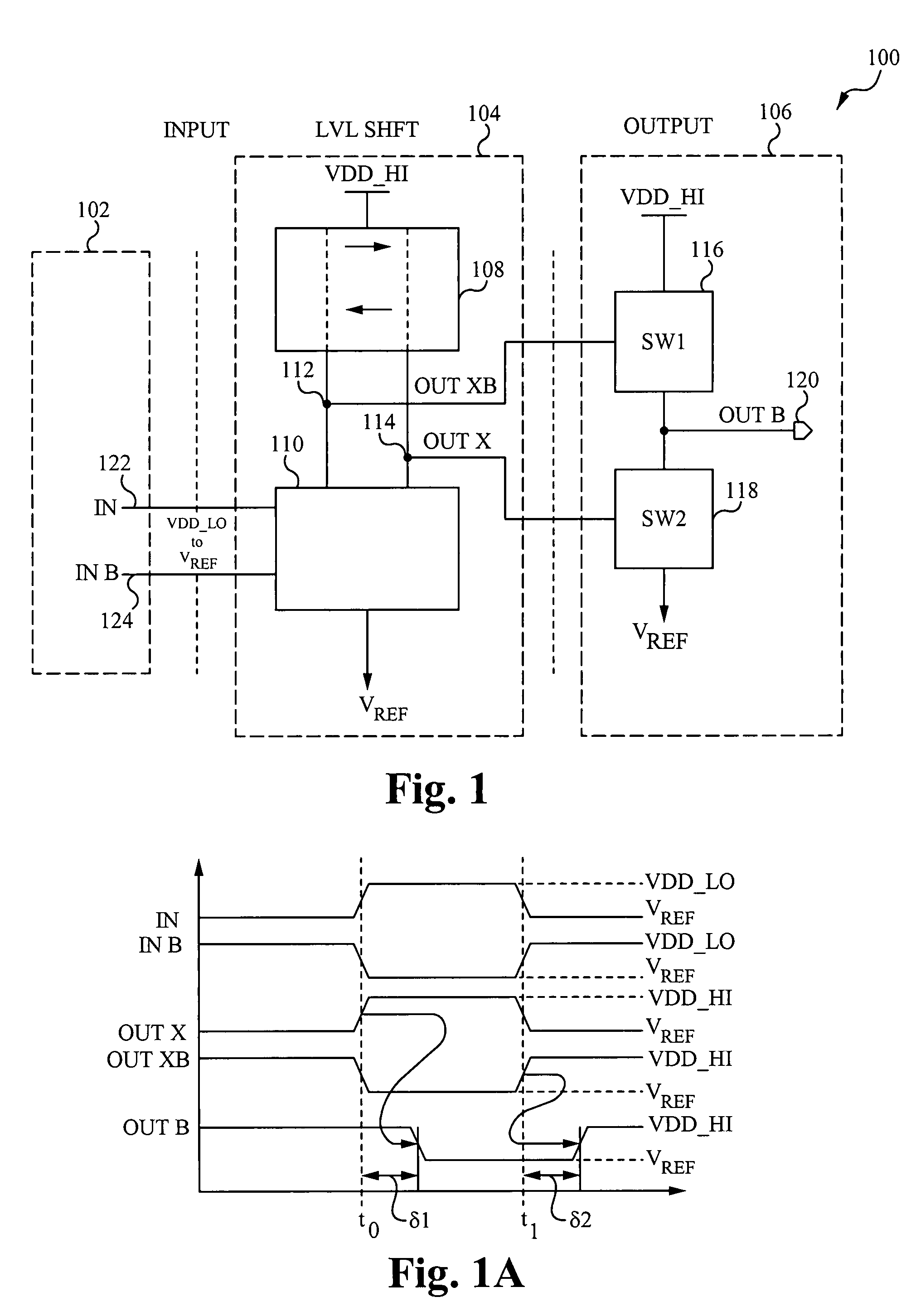
[0023]Referring now to FIG. 1, a level shifting circuit according to a first embodiment is shown in a block schematic diagram and designated by the general reference character 100. A level shifting circuit 100 can include an input stage 102, a shift stage 104, and an output stage 106. Input stage 102 can include input paths 122, 124. Input paths 122, 124 can carry signals that vary within a first voltage range, which in this particular example is shown to be between a non-shifted high power supply voltage VDD_LO and a reference voltage VREF.

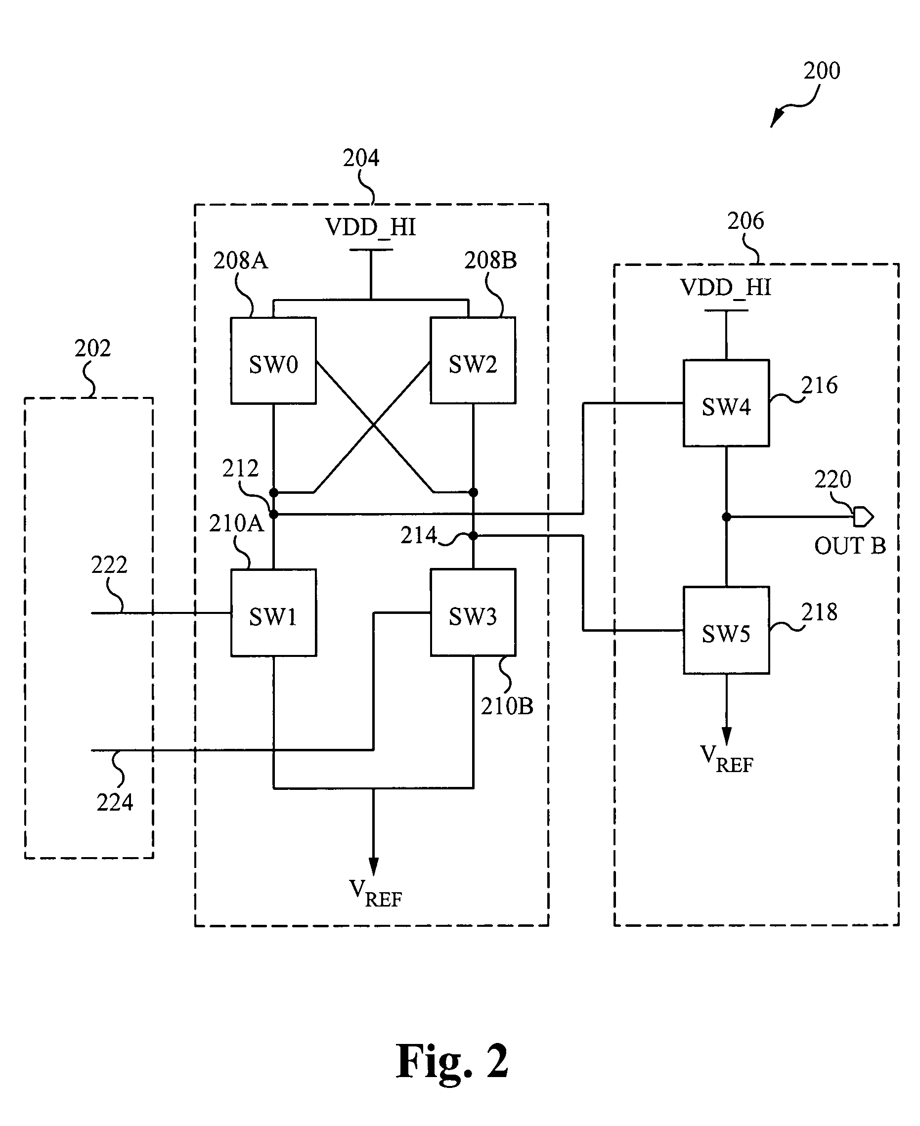
[0024]Shift stage 104 can include a high voltage section 108, low voltage section 110, a first internal node 112 and a second internal node 114. S...


PUM


Abstract

A level shifting circuit can include a shift stage that latches first and second internal nodes to opposite shifted logic potentials in response to different transitions at an input signal node. The input signal node can vary between non-shifted logic potentials. An output stage can enable a first controllable impedance path coupled between an output node and a first shifted power supply node in response to a first type transition at the first internal node, and can enable a second controllable impedance path coupled between the output node and a second shifted power supply node in response to the first type transition at the second internal node.

Description

TECHNICAL FIELD[0001]The present invention relates generally to level shifting circuits, and more particularly to level shifting circuits that can produce shifted signal levels with balanced rise and fall delays.BACKGROUND OF THE INVENTION[0002]Level shifting circuits can shift an input signal, that transitions between a first voltage range, into an output signal that transitions between a second voltage range, that can be greater or smaller than the first voltage range. Level shifting operations are typically utilized to allow one signal, generated in one voltage domain (i.e., range), to drive circuits operating in another voltage domain. For applications in which level shifters are included in timing signal paths, ensuring predictable signal delays can present design challenges.[0003]To better understand various features of the disclosed embodiments, a conventional level shifting circuit will now be described.[0004]Referring now to FIG. 9, a conventional level shifting circuit is ...

Claims


Application Information

Patent Timeline
Patent Type & Authority Patents(United States)
IPC IPC(8): H03L5/00
CPCH03K3/356113H03K3/356165H03K19/018521
Inventor KOTTAPALLI, VENKATA ANIL
Owner AVAGO TECH INT SALES PTE LTD
Why Eureka
Try Eureka