Solid-state imaging device and drive control method for the same

a technology of solid-state imaging and drive control, which is applied in the direction of radioation control devices, instruments, television systems, etc., to achieve the effects of reducing saturation shading, increasing the transition time, and reducing saturation shading

Inactive Publication Date: 2005-01-06
SONY CORP
View PDF6 Cites 28 Cited by
  • Summary
  • Abstract
  • Description
  • Claims
  • Application Information

AI Technical Summary

Benefits of technology

[0034] A first solid-state imaging device according to the invention is a solid-state imaging device arranged for implementing the foregoing drive control method of the invention. The drive voltage to the drain line can be driven by being blunted such that, when a drive pulse is applied to the drain drive buffer, the off transition time on a voltage waveform in driving the drain line is longer (preferably, in a range of five times or greater and ten thousand times or smaller, more preferably 50 to 600 times) than the off transition time on any of the reset line to be driven by a reset drive buffer and the transfer line to be driven by the transfer drive buffer. Incidentally, the transition time of a drive pulse itself to be applied to each drive buffer may be made as a “pulse” in a general concept having a fall and rise fully shortened.
[0038] Meanwhile, a second solid-state imaging device of the invention is a solid-state imaging device having unit pixels structured by including a charge generating section for generating a signal charge commensurate with a received light and three transistors wherein, by making negative the low level voltage of the gate of a read select transistor, a potential barrier is formed to prevent the charge from leaking from the charge generating section to the charge storing part (corresponding to the improve technique based on the second approach in the embodiment, referred later). Incidentally, the voltage is given in a magnitude of range not to cause breakdown. Meanwhile, the off voltage is preferably set with a negative voltage in a magnitude capable of generating a hole channel at an interface of a semiconductor structuring the unit pixels. With a variable setting voltage, the arrangement is more preferable.
[0043] For example, the technique based on the first approach has been made by finding points, i.e. saturation shading is reduced by increasing the transition time (e.g. fall time in switching over to the low, on the NMOS sensor) in turning off the voltage to the drain line common to all the pixels, the optimal value thereof exits under certain device drive condition, and so on. For example, applied is a technique of making proper the W / L ratio of a transistor structuring the drive buffer or making proper the operation current during drive by inserting a control resistance or current source between reference voltages. Due to this, the transition time in turning off the drain voltage is increased longer than the transition time in turning off any of the reset line and the transfer line, preferably five times or greater and ten thousand times or smaller. This makes uniform the characteristic between the pixels at the periphery and at the center, thereby reducing saturation shading.
[0044] Meanwhile, the technique based on the second approach can make the potential barrier high relative to the charge storing part by deepening (switching toward the negative, if on the NMOS sensor) the electrode voltage during turning off the read select transistor than a master reference voltage (e.g. GND level) regulating the reference voltage over the pixel entirety, thereby reducing saturation shading.
[0045] Meanwhile, the technique based on the third approach has been made by finding the point that the fluctuation of well potential can be suppressed by providing a bias line for fixing the well potential, making it possible to reduce shading.
[0046] Meanwhile, the technique based on the fourth approach has been made by finding the point that, by making in a depression type the reset transistor of the reset section structuring the unit pixel, leak current is suppressed to a charge storing part such as the floating diffusion thereby broadening the dynamic range at the charge storing part.

Problems solved by technology

The two problems and analysis results are the new matters not to exist on the CMOS sensor of a type to select every pixel by the vertical select transistor 40.

Method used


Image

  • Solid-state imaging device and drive control method for the same
  • Solid-state imaging device and drive control method for the same
  • Solid-state imaging device and drive control method for the same

Examples


Embodiment Construction

[0067] Now embodiments of the present invention will be explained in detail with reference to the drawings. Note that the below exemplifies the application to a CMOS imaging device, an example of an X-Y addressing solid-state imaging device. Meanwhile, the CMOS imaging device is explained on the assumption that all the pixels are configured by the NMOS.

[0068]

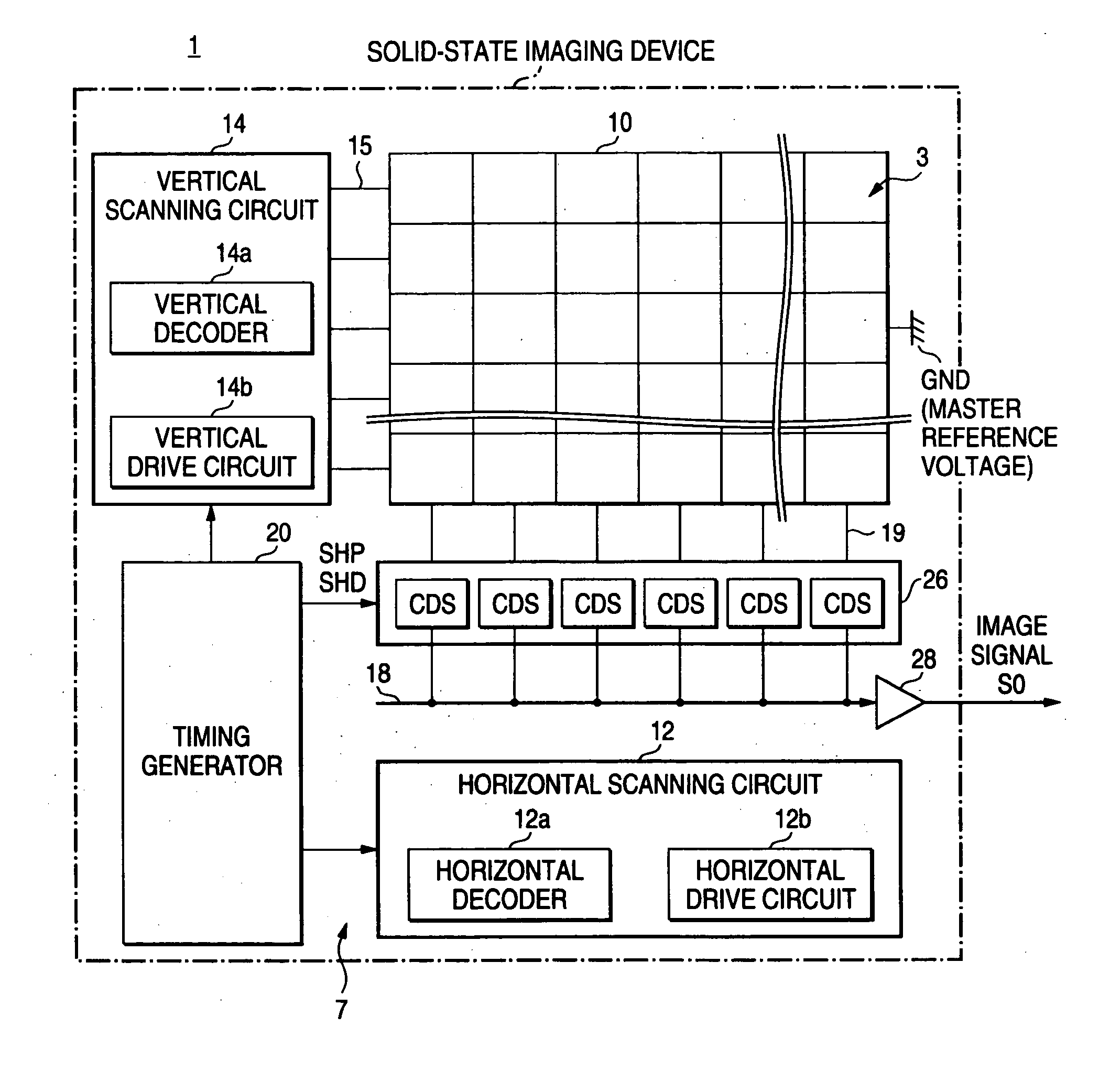
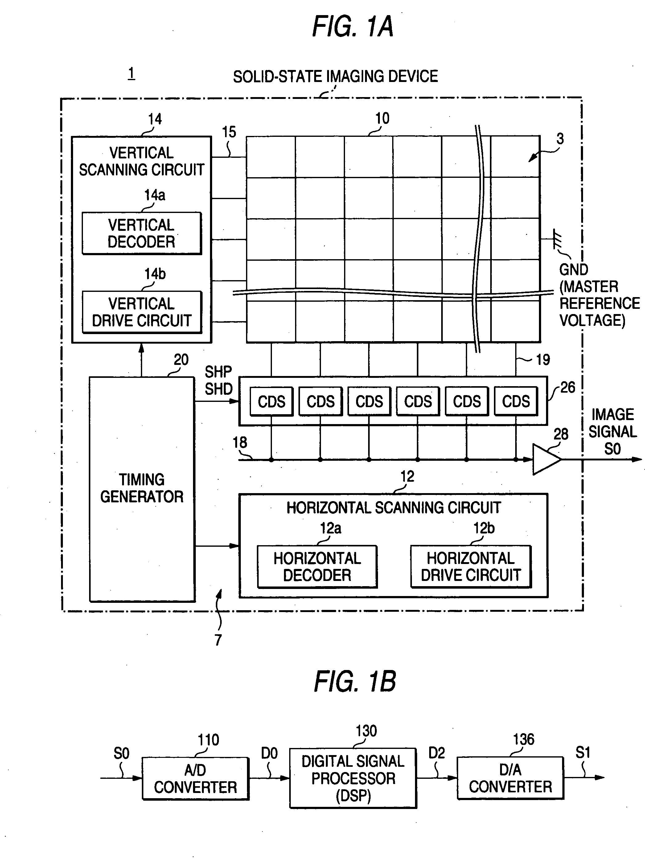
[0069]FIG. 1 is a schematic arrangement diagram of a CMOS solid-state imaging device according to an embodiment of the present invention. The solid-state imaging device 1 is applicable as an electronic still camera capable of imaging for color pictures. For example, in a still-picture imaging mode, setting is made to a mode for reading all the pixels.

[0070] The solid-state imaging device 1 has an imaging section arranged, on rows and columns, with pixels (i.e. in two-dimensional matrix form) including light-receiving elements to output a signal commensurate with the amount of incident light, providing an signal output, or volt...


PUM


Abstract

A CMOS sensor has unit pixels each structured by a light receiving element and three transistors, to prevent against the phenomenon of saturation shading and the reduction of dynamic range. The transition time (fall time), in switching off the voltage on a drain line shared in all pixels, is given longer than the transition time in turning of any of the reset line and the transfer line. For this reason, the transistor constituting a DRN drive buffer is made proper in its W / L ratio. Meanwhile, a control resistance or current source is inserted on a line to the GND, to make proper the operation current during driving. This reduces saturation shading amount. By making a reset transistor in a depression type, the leak current to a floating diffusion is suppressed to broaden the dynamic range.

Description

BACKGROUND OF THE INVENTION [0001] 1. Technical Field of the Invention [0002] The present invention relates to a solid-state imaging device arranged with a plurality of unit pixels so that a signal can be desirably selected and read out of the individual unit pixel under address control, and to a control method for the same. More particularly, the invention relates to a solid-state imaging device of a type having unit pixels each structured by a photoelectric converter element and three transistors without having a select transistor, and to a drive control method for the same. [0003] 2. Description of the Related Art [0004] The amplification-type solid-state imaging device (APS: Active Pixel Sensor, also called a gain cell) as one kind of X-Y addressing solid-state imaging device is structured with pixels by the use of active elements (MOS transistors) such as the MOS structure, in order to provide the pixel with an amplification function. Namely, the signal charge (photoelectrons),...

Claims


Application Information

Patent Timeline
Patent Type & Authority Applications(United States)
IPC IPC(8): H04N5/335H01L27/146H04N5/355H04N5/361H04N5/369H04N5/374H04N5/376
CPCH04N5/3559H04N5/365H04N5/37213H04N5/376H04N5/374H04N25/59H04N25/67H04N25/74H04N25/76A47J19/06A47J19/02A47J43/07H04N25/75H04N23/54H04N25/709H04N25/713H04N25/745
Inventor MABUCHI, KEIJIFUNATSU, EIICHIKASAI, MASANORI
Owner SONY CORP
Why Eureka
Try Eureka