Semiconductor memory device having on-die-termination device and operation method thereof

a memory device and memory technology, applied in the direction of digital storage, instruments, circuit coupling arrangements, etc., can solve the problems of terminal resistor not being turned on/off, difficult to properly achieve resistance matching, signal transmission error, etc., to achieve the effect of stably securing an on-die-termination (odt) latency

Active Publication Date: 2009-01-15
SK HYNIX INC
View PDF11 Cites 59 Cited by
  • Summary
  • Abstract
  • Description
  • Claims
  • Application Information

AI Technical Summary

Benefits of technology

[0033]Embodiments of the present invention are directed to providing a semiconductor memory device capable of stably securing an on-die-termination (ODT) latency in spite of PVT variations and various operating speeds.

Problems solved by technology

However, if a resistance matching between the devices is not proper, a transmission signal may be reflected, thus leading to an error in signal transmission.
Specially, when a fixed resistor is connected externally to the memory device, it is difficult to properly achieve the resistance matching because a resistance of the termination resistor in the memory device could be changed due to several factors such as aging of an integrated circuit (IC), temperature variation or difference in fabrication process.
According to the conventional art, however, the start flag signal or the end flag signal may not be positioned within the counting window due to PVT (process, voltage and temperature) variations even though the ODT replica is designed to have the optimized delay time, thus leading to such a malfunction that the terminal resistor is not turned on / off at a time point set by standard specification.

Method used


Image

  • Semiconductor memory device having on-die-termination device and operation method thereof
  • Semiconductor memory device having on-die-termination device and operation method thereof
  • Semiconductor memory device having on-die-termination device and operation method thereof

Examples


Embodiment Construction

[0047]Hereinafter, a semiconductor memory device having an on-die-termination (ODT) device and an operation method thereof in accordance with the present invention will be described in detail with reference to the accompanying drawings.

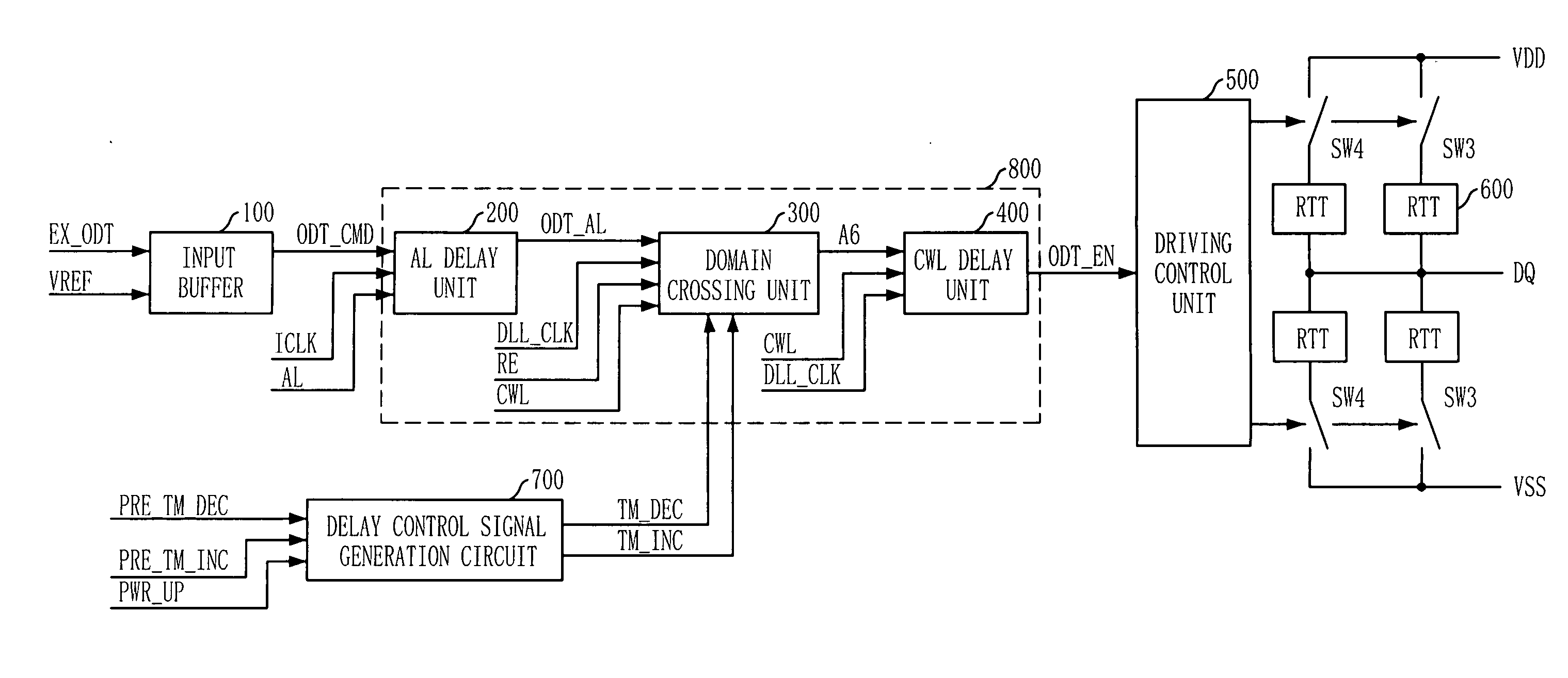
[0048]FIG. 4 illustrates a block diagram of a semiconductor memory device having an ODT device in accordance with an embodiment of the present invention.

[0049]Referring to FIG. 4, the semiconductor memory device in accordance with the present invention includes an input buffer 100, a delay path unit 800, a delay control signal generation unit 700, a plurality of termination resistors 600 and switches SW, and a driving control unit 500. The input buffer 100 is configured to receive an external ODT command EX_ODT to output an ODT command ODT_CMD. The delay path unit 800 is configured to delay the ODT command ODT_CMD by a predetermined delay time corresponding to an ODT latency to output a driving control signal ODT_EN, and configured to convert the ODT ...


PUM


Abstract

A semiconductor memory device is capable of stably securing an on-die-termination (ODT) latency in spite of PVT variations and various operating speeds. The semiconductor memory device includes a plurality of termination resistors connected to an output pad in series and parallel, a drive controller, a delay path, and a delay control signal generator. The drive controller activates/inactivates the plurality of termination resistors in response to a driving control signal. The delay path delays a termination command by a delay time corresponding to an on-die-termination (ODT) latency to output the driving control signal, wherein the termination command is converted into a delay locked loop (DLL) clock domain signal. The delay control signal generator controls a conversion point of the termination command into the DLL clock domain signal.

Description

CROSS-REFERENCE TO RELATED APPLICATIONS[0001]The present invention claims priority to Korean patent application number 10-2007-0070052, filed on Jul. 12, 2007, which is incorporated by reference in its entirety.BACKGROUND OF THE INVENTION[0002]The present invention relates to semiconductor design technology, and more particularly to a semiconductor memory device having an on-die-termination device.[0003]Generally, many new concepts have been proposed to rapidly control data transmission rate in double data rate (DDR) memory devices. Among the various concepts, the use of a termination resistor makes the memory device easily transmit signals with external devices.[0004]However, if a resistance matching between the devices is not proper, a transmission signal may be reflected, thus leading to an error in signal transmission. Specially, when a fixed resistor is connected externally to the memory device, it is difficult to properly achieve the resistance matching because a resistance of...

Claims


Application Information

Patent Timeline
Patent Type & Authority Applications(United States)
IPC IPC(8): G11C7/00
CPCG11C7/1078G11C7/109G11C7/1093G11C7/1075G11C7/1045G11C7/1057G11C7/1066G11C7/1009G11C7/20G11C7/22H03K19/017545
Inventor KIM, KYUNG-WHAN
Owner SK HYNIX INC
Why Eureka
Try Eureka