

Design method and design apparatus for semiconductor integrated circuit
a technology of integrated circuits and design methods, applied in the direction of instruments, computing, electric digital data processing, etc., can solve the problems of increasing the closure period deterioration of timing and wiring, and increasing the number of steps required, so as to prevent the occurrence of wire congestion and reduce the number of steps
- Summary
- Abstract
- Description
- Claims
- Application Information
AI Technical Summary
Benefits of technology
Problems solved by technology
Method used
Image

Examples
first embodiment
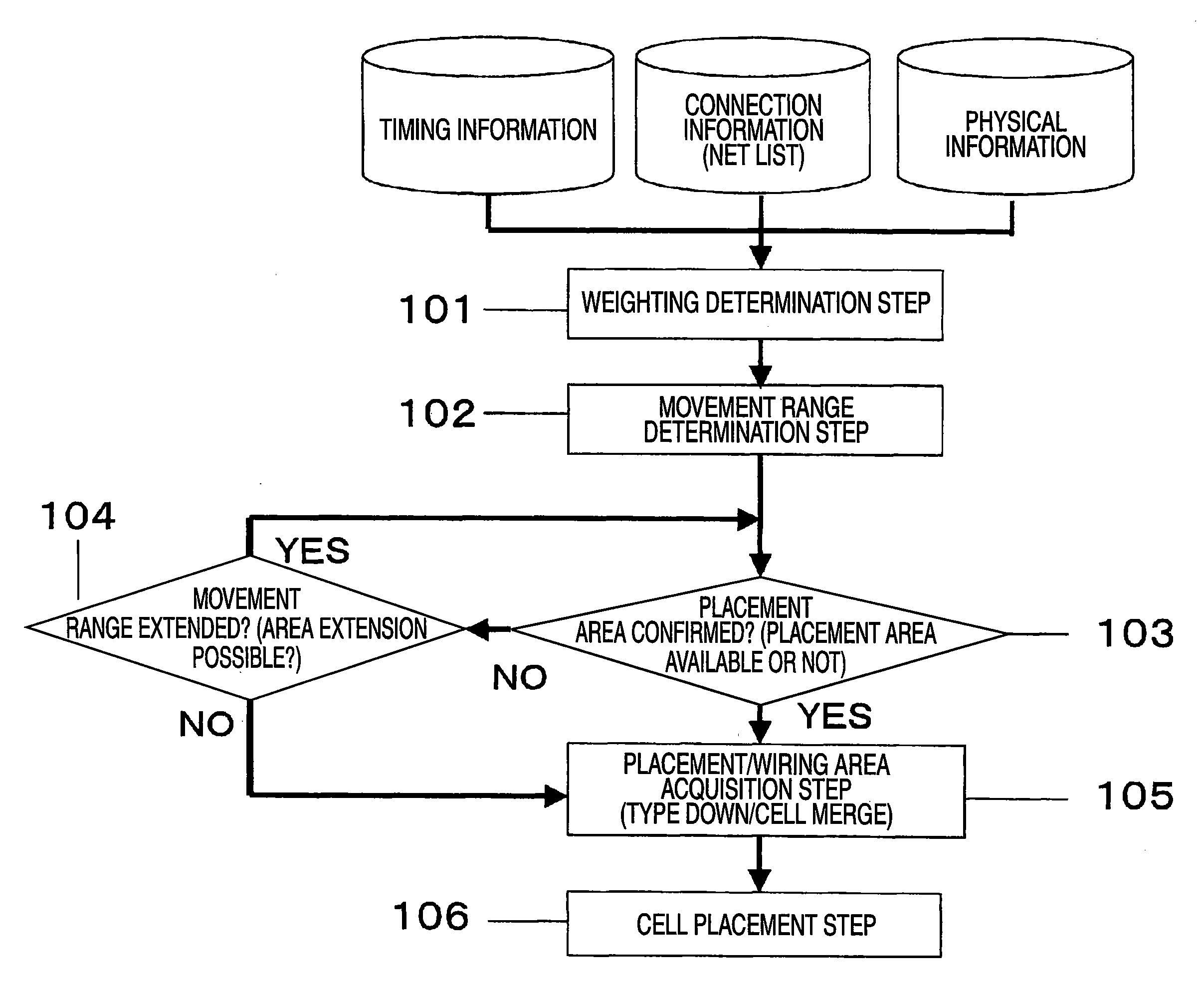
[0083]FIG. 1 is a flowchart showing a design method, according to a first embodiment of the present invention, that includes a cell placement method for a semiconductor integrated circuit. This method is characterized by including: a weight determination step 101 of receiving timing information and connection information (hereinafter referred to as a net listing) and of performing a weighting calculation process, while regarding a cell having a small timing margin as a cell that has a greatly enhanced weight, so that movement ranges for cells are reduced when the weightings of the cells are increased; and a cell placement step 106 of employing the results obtained at the weight determination step to place cells. This cell placement step includes the following processing. Weighting of cells is performed while a cell having not only a small timing margin but also an extended Manhattan distance, obtained based on received physical information, is regarded as a cell having a greatly enh...
second embodiment
[0103]A second embodiment of the present invention will now be described.
[0104]In the first embodiment, cells are weighted based on the timing margin, the Manhattan distance and the number of fanouts, and the obtained weights are added to perform cell placement. According to the second embodiment, the weighting calculation process is performed based only on a timing margin, and cells are to be placed using only the weighting results.
[0105]FIG. 18 is a flowchart showing the weight determination processing performed in the second embodiment. The weight determination processing is the same as that in FIG. 4 for the first embodiment, except that the step 202 of calculating the number of fanouts and the step 203 of calculating the Manhattan distance are not included, and the contents of the weighting determination step 204 are different.
[0106]While referring to FIG. 18, the weight determination processing for the second embodiment includes: a step 701 of calculating a timing margin based...
third embodiment
[0108]A third embodiment of the present invention will now be described.
[0109]In the first embodiment, cells are weighted based on the timing margin, the Manhattan distance and the number of fanouts, and the obtained weights are added to perform cell placement. In the third embodiment, an explanation will be given for a case wherein the weighting calculation process is performed based only on a timing margin and a Manhattan distance, and cells are to be placed based on the weighting results.
[0110]FIG. 19 is a flowchart showing the weight determination processing performed for the third embodiment. The weight determination processing is the same as that shown in FIG. 4 for the first embodiment, except that the step 202 of calculating the number of fanouts is not included, and the contents of the weight determination step 204 are different.
[0111]While referring to FIG. 19, the weight determination processing for this embodiment includes: a step 801 of calculating a timing margin based...
PUM
 Abstract
Description
Claims
Application Information