

Electronic component package and method of manufacturing same
a technology of electronic components and manufacturing methods, applied in the direction of electrical equipment, semiconductor devices, semiconductor/solid-state device details, etc., can solve the problems of difficult to respond to alterations to specifications flexibly and quickly, difficult to manufacture multi-chip modules through this method, and difficult to mass-produce electronic component packages at low cost in a short period of time. , to achieve the effect of low cost, short period of time, and high integration
- Summary
- Abstract
- Description
- Claims
- Application Information
AI Technical Summary
Benefits of technology
Problems solved by technology
Method used
Image

Examples
Embodiment Construction
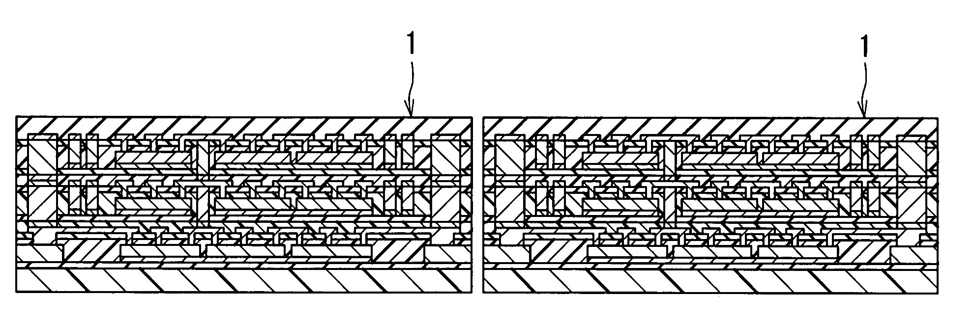
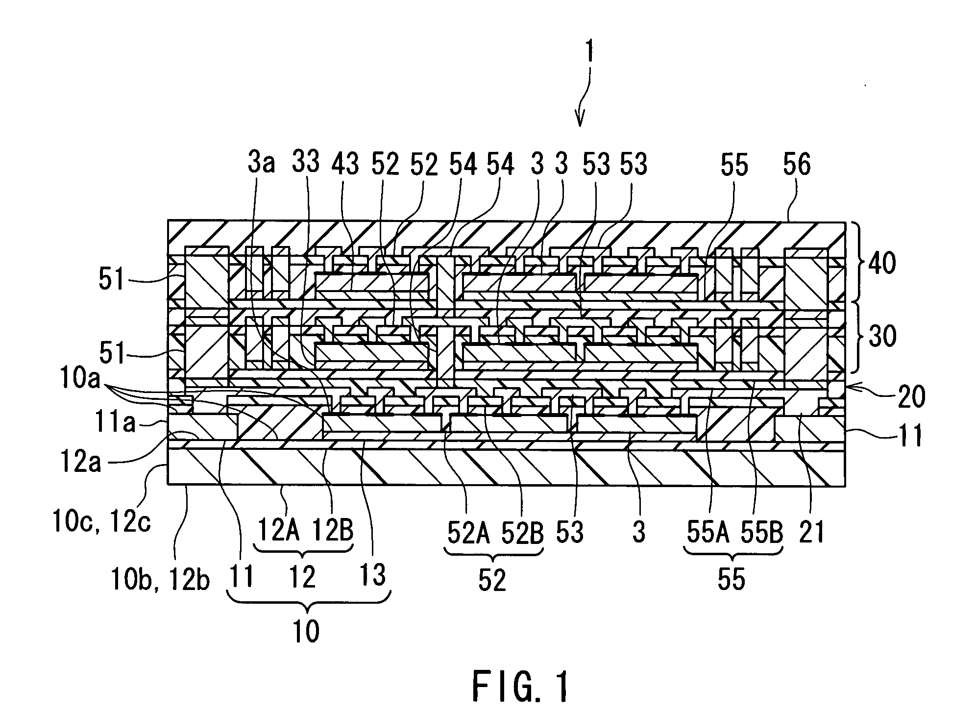
[0077]An embodiment of the present invention will now be described in detail with reference to the drawings. Reference is first made to FIG. 1 to describe the configuration of an electronic component package of the embodiment. FIG. 1 is a cross-sectional view of the electronic component package of the embodiment. As illustrated in FIG. 1, the electronic component package 1 of the embodiment includes a base 10 and a plurality of layer portions stacked on the base 10. FIG. 1 illustrates an example in which the electronic component package 1 includes three layer portions 20, 30 and 40. In this example, the layer portions 20, 30 and 40 are stacked in this order on the base 10. Alternatively, the number of the plurality of layer portions that the electronic component package 1 includes may be two, or may be equal to or greater than four. The electronic component package 1 is rectangular-solid-shaped, for example. In this case, the base 10 has a top surface 10a, a bottom surface 10b, and ...
PUM
 Abstract
Description
Claims
Application Information