Method for integrating silicon-on-nothing devices with standard CMOS devices

Active Publication Date: 2009-02-05
STMICROELECTRONICS SRL +1
View PDF5 Cites 35 Cited by
  • Summary
  • Abstract
  • Description
  • Claims
  • Application Information

AI Technical Summary

Benefits of technology

[0009]Another embodiment of the present invention provides an integrated circuit including transistors of first and second types in a single substrate. The integrated circuit includes a first active zone of the substrate and a second active zone of the substrate delimited by lateral isolation trench regions, a first layer of dielectric material located on the second active zone, and a second layer of semiconductor material located on the first layer. An upper surface of the second active zone is below an upper surface of the first active zone, and an upper surface of the second layer i

Problems solved by technology

The presence of a thick substrate that is electrically continuous with the active superficial layers, however, induces parasitic phenomena therein, and makes them sensitive in particular to electrical disturbances (for example, leakage currents toward the substrate).

Method used


Image

  • Method for integrating silicon-on-nothing devices with standard CMOS devices
  • Method for integrating silicon-on-nothing devices with standard CMOS devices
  • Method for integrating silicon-on-nothing devices with standard CMOS devices

Examples


Embodiment Construction

[0013]Preferred embodiments of the present invention will be described in detail hereinbelow with reference to the attached drawings.

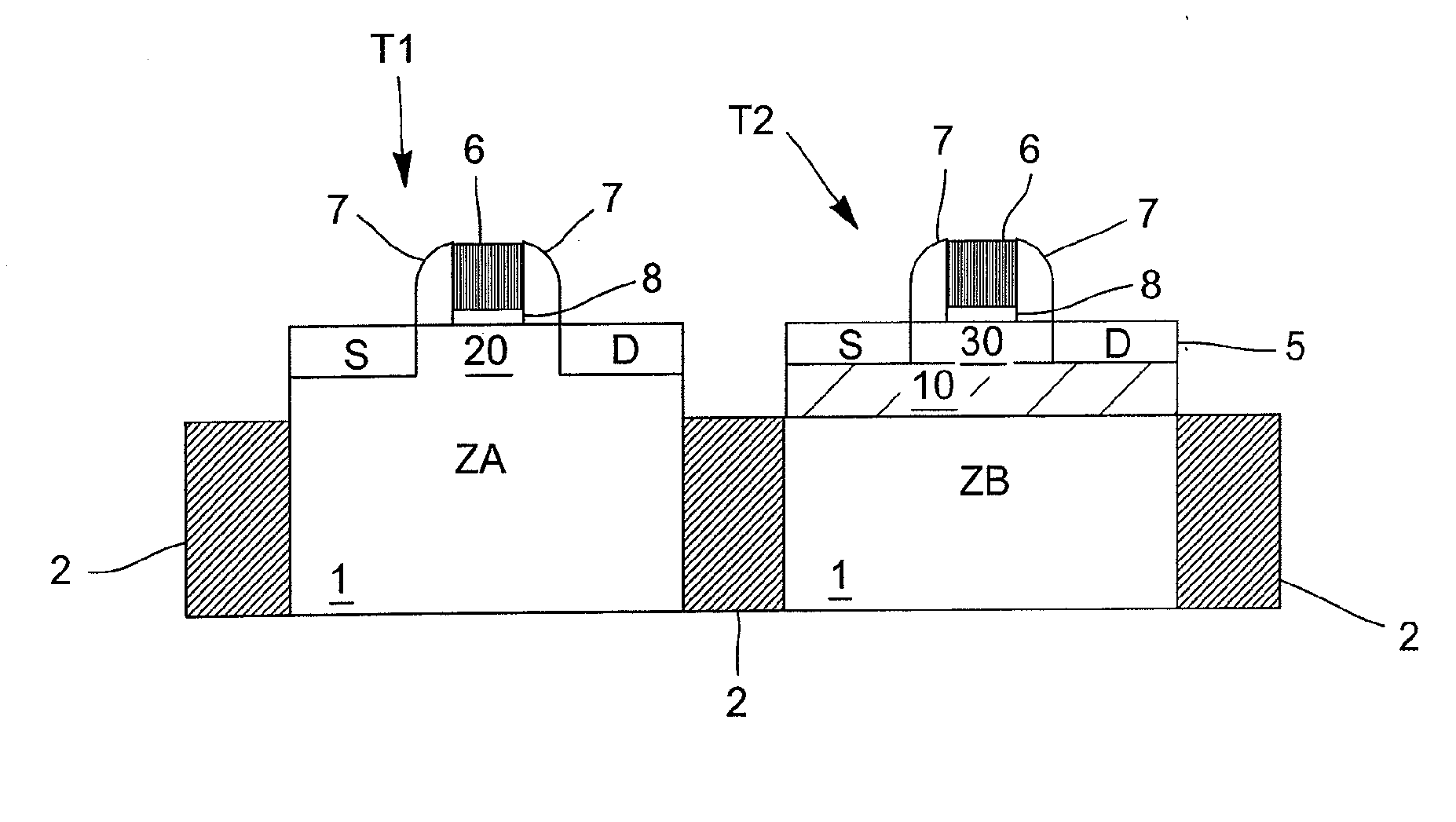
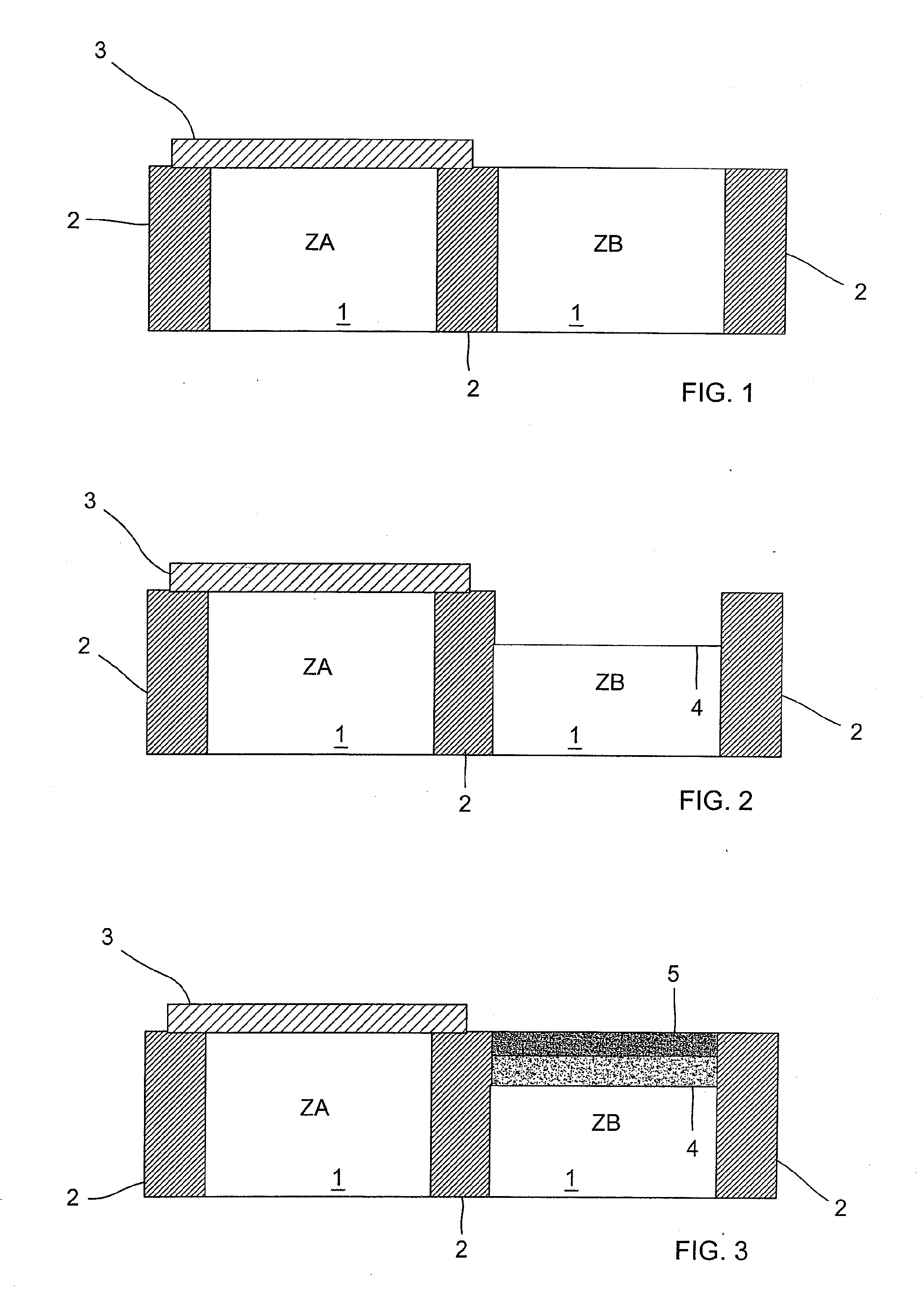
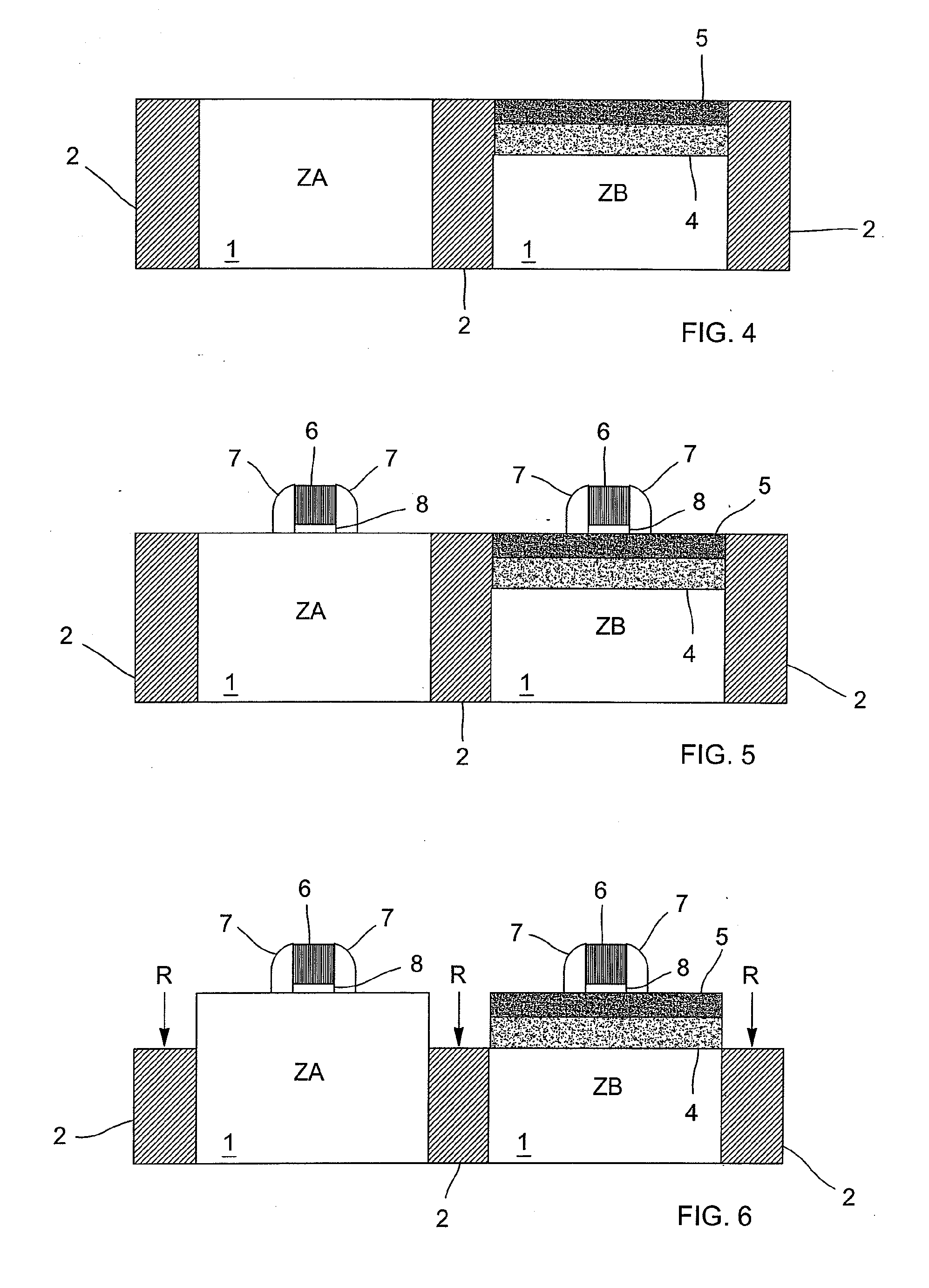
[0014]Preferred embodiments of the present invention provide a method for fabricating transistors of first and second types in a single substrate. At least one first active zone and at least one second active zone of the substrate are delimited by lateral isolation trench regions, and an upper portion of the second active zone is removed so that an upper surface of the second active zone is below an upper surface of the first active zone. After removing the upper portion of the second active zone, first and second layers of semiconductor material are formed on the second active zone, so that an upper surface of the second layer is substantially in the same plane as the upper surface of the first active zone. The first layer is constituted by a first material that is selectively removable with respect to a second material constituting the second active ...


PUM


Abstract

A method is provided for fabricating transistors of first and second types in a single substrate. First and second active zones of the substrate are delimited by lateral isolation trench regions, and a portion of the second active zone is removed so that the second active zone is below the first active zone. First and second layers of semiconductor material are formed on the second active zone, so that the second layer is substantially in the same plane as the first active zone. Insulated gates are produced on the first active zone and the second layer. At least one isolation trench region is selectively removed, and the first layer is selectively removed so as to form a tunnel under the second layer. The tunnel is filled with a dielectric material to insulate the second layer from the second active zone of the substrate. Also provided is such an integrated circuit.

Description

CROSS-REFERENCE TO RELATED APPLICATIONS[0001]This application is based upon and claims priority from French Patent Application No. 07 04870, filed Jul. 5, 2007, the entire disclosure of which is herein incorporated by reference.FIELD OF THE INVENTION[0002]The present invention relates in general to the field of integrated semiconductor circuits, and more specifically to a method for integrating conventional “bulk” CMOS transistors with transistors having a thin conductive channel on insulator according to a silicon-on-nothing (SON) or localized silicon-on-insulator (SOI) structure.BACKGROUND OF THE INVENTION[0003]In the case of a conventional MOS transistor in “bulk” technology, the active zones are directly implanted in a mass (“bulk”) of thick silicon forming the substrate. The presence of a thick substrate that is electrically continuous with the active superficial layers, however, induces parasitic phenomena therein, and makes them sensitive in particular to electrical disturban...

Claims


Application Information

Patent Timeline
IPC IPC(8): H01L21/336H01L29/786
CPCH01L21/823412H01L21/823481H01L21/823807H01L27/1207H01L21/84H01L27/1203H01L21/823878
Inventor LOUBET, NICOLASDUTARTRE, DIDIERMONFRAY, STEPHANE
Owner STMICROELECTRONICS SRL
Why Eureka
Try Eureka