Method and configuration for connecting test structures or line arrays for monitoring integrated circuit manufacturing

a test structure and integrated circuit technology, applied in semiconductor/solid-state device testing/measurement, semiconductor/solid-state device details, instruments, etc., can solve problems such as easy to fail, systematic faults, and difficult or impossible to place all those test structures on a single test chip

Active Publication Date: 2009-02-05
PDF SOLUTIONS INC
View PDF4 Cites 86 Cited by
  • Summary
  • Abstract
  • Description
  • Claims
  • Application Information

AI Technical Summary

Benefits of technology

[0018]In some embodiments, a test chip comprises at least one level having an array of regions. Each region is capable of including at least one test structure. At least some of the regions include respective test structures. The level has a plurality of driver lines that provide input signals to the test structures. The level has a plurality of receiver lines that receive output signals from the test structures. The...

Problems solved by technology

Random defects (e.g. particles) can cause electrically measurable faults (killer defects), which are dependent on the chip layout as well as the layer and location of the defects.
Also, certain layout geometries can cause systematic faults dependent on specific combinations of layout and manufacturing process steps.
Random as well as systematic faults are responsible for manufacturing related malfunction of chips.
It is difficult or impossible to place all those test structures on a single test chip if they are all connected to individual pads for testing, since there is not enough area to place all those pads.
If one were to place differently designed test structures within such an array, the test procedure would fail.
The array also does not allow any fast digital testing.
This technique is of no help, if differently designed test structures have to be placed on a test chip.
None of the methods mentioned above, allow stacking of structures in multiple layers on top of each other to efficiently make use of 10 or more routing layers that are commonly used in semiconductor manufacturing.
Also, all these arrays are only able to investigate open circuit faults and are of no use if also short circuits have to be investigated.
Unfortunately, these methods are limited to short circuits only and they have problems in disentangling multiple faults, if they occur in more than one test structures as it has ...

Method used


Image

  • Method and configuration for connecting test structures or line arrays for monitoring integrated circuit manufacturing
  • Method and configuration for connecting test structures or line arrays for monitoring integrated circuit manufacturing
  • Method and configuration for connecting test structures or line arrays for monitoring integrated circuit manufacturing

Examples


Embodiment Construction

[0040]U.S. Provisional Patent Application No. 60 / 511,535, filed Oct. 15, 2003 is incorporated by reference herein in its entirety, as though fully set forth herein.

[0041]This description of the exemplary embodiments is intended to be read in connection with the accompanying drawings, which are to be considered part of the entire written description. In the description, relative terms such as “lower,”“upper,”“right,”“left,”“horizontal,”“vertical,”, “above,”“below,”“up,”“down,”“top” and “bottom” as well as derivative thereof (e.g., “horizontally,”“downwardly,”“upwardly,” etc.) should be construed to refer to the orientation as then described or as shown in the drawing under discussion. These relative terms are for convenience of description and do not require that the apparatus be constructed or operated in a particular orientation.

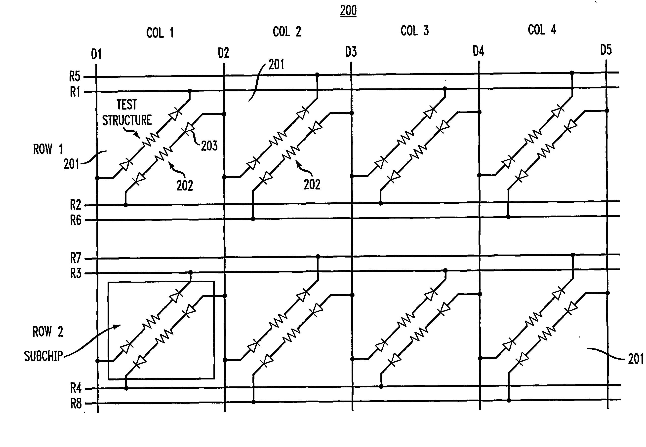
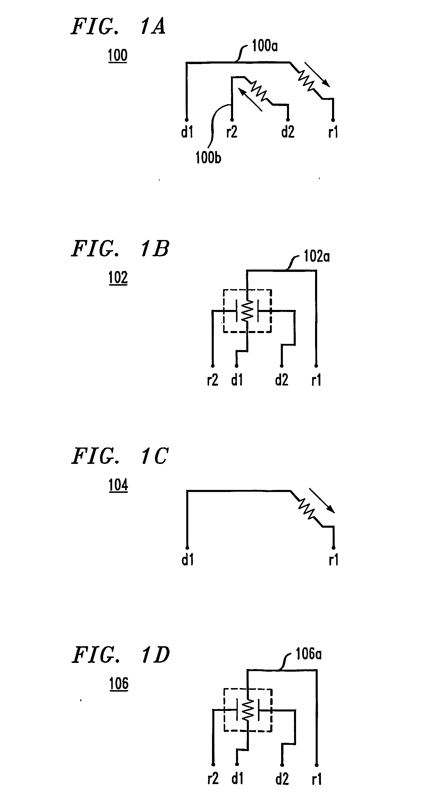
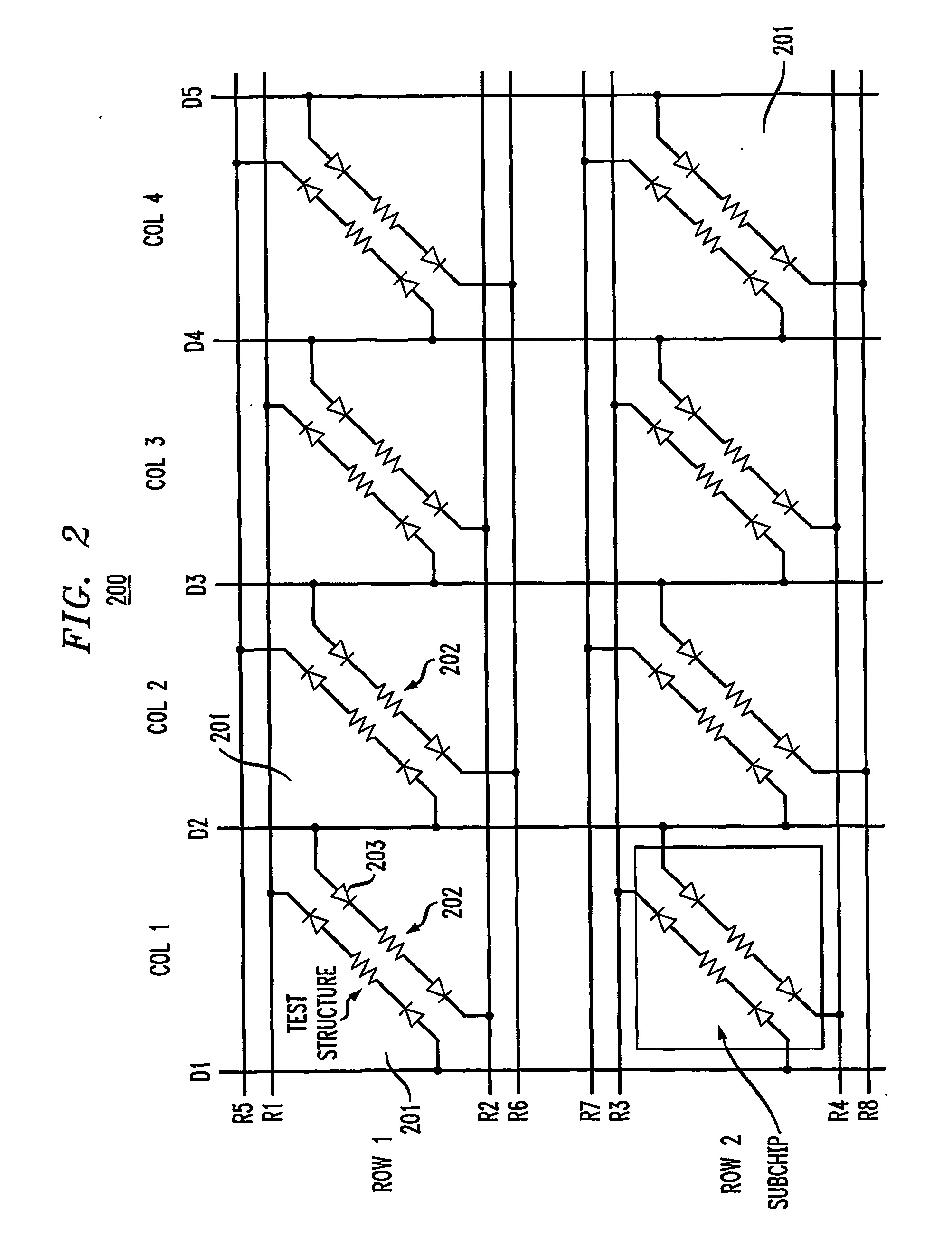
[0042]To characterize multi layer semiconductor manufacturing processes it is not necessarily required to introduce or invent novel test structures to dete...


PUM


Abstract

A test chip comprises at least one level having an array of regions. Each region is capable of including at least one test structure. At least some of the regions include respective test structures. The level has a plurality of driver lines that provide input signals to the test structures. The level has a plurality of receiver lines that receive output signals from the test structures. The level has a plurality of devices for controlling current flow. Each test structure is connected to at least one of the driver lines with a first one of the devices in between. Each test structure is connected to at least one of the receiver lines with a second one of the devices in between, so that each of the test structures can be individually addressed for testing using the driver lines and receiver lines.

Description

[0001]This application claims the benefit of U.S. Provisional Patent Application No. 60 / 511,535, filed Oct. 15, 2003.FIELD OF THE INVENTION[0002]This invention relates to methods for measuring and evaluating the process and design related statistical variations of an integrated circuit manufacturing process in order to determine their sources and their effects on the yield and performance of the product.BACKGROUND[0003]Random defects (e.g. particles) can cause electrically measurable faults (killer defects), which are dependent on the chip layout as well as the layer and location of the defects. Also, certain layout geometries can cause systematic faults dependent on specific combinations of layout and manufacturing process steps. Random as well as systematic faults are responsible for manufacturing related malfunction of chips. So, investigating random and systematic faults is important for yield enhancement and to control quality of process steps and product chips, as discussed in...

Claims


Application Information

Patent Timeline
IPC IPC(8): G06F19/00G06F
CPCG01R31/2884H01L22/34H01L2924/3011H01L2924/0002H01L2924/00H01L22/00
Inventor HESS, CHRISTOPHERGOLDMAN, DAVID
Owner PDF SOLUTIONS INC
Why Eureka
Try Eureka