Air-gap grapheme transistor and manufacturing method thereof

A graphene and air-gap technology, applied in semiconductor/solid-state device manufacturing, electrical components, semiconductor devices, etc., can solve the problem of reducing graphene carrier mobility, degrading the electrical properties of graphene transistors, and inability to deposit gate dielectrics, etc. question

Inactive Publication Date: 2011-05-25
FUDAN UNIV
View PDF3 Cites 29 Cited by
  • Summary
  • Abstract
  • Description
  • Claims
  • Application Information

AI Technical Summary

Problems solved by technology

[0004] At present, graphene transistors still face two main problems: 1) the bandgap width of graphene is zero; 2) since the surface of graphene is basically chemically inert except for the edge, it is impossible to use atomic layer deposition method on graphene Direct Depo...

Method used


Image

  • Air-gap grapheme transistor and manufacturing method thereof
  • Air-gap grapheme transistor and manufacturing method thereof
  • Air-gap grapheme transistor and manufacturing method thereof

Examples


Embodiment Construction

[0031] Exemplary embodiments of the present invention will be described in detail below with reference to the accompanying drawings. In the drawings, the thicknesses of layers and regions are exaggerated for convenience of illustration, and the shown sizes do not represent actual sizes. The referenced figures are schematic illustrations of idealized embodiments of the invention, and the illustrated embodiments of the invention should not be construed as limited to the particular shapes of regions illustrated in the figures but are to include resulting shapes, such as manufacturing-induced deviations. The representations in the figures are schematic, but this should not be considered as limiting the scope of the invention. Meanwhile, in the following description, the term substrate used can be understood to include the semiconductor substrate being processed, possibly including other thin film layers prepared thereon.

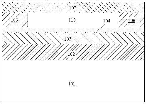
[0032] figure 1 An embodiment of the air-gap graphene tr...


PUM

PropertyMeasurementUnit
Thicknessaaaaaaaaaa
Thicknessaaaaaaaaaa
Thicknessaaaaaaaaaa

Abstract

The invention belongs to the technical field of carbon integrated circuit manufacturing, in particular relates to an air-gap grapheme transistor and a manufacturing method thereof. In the method, gate electrodes and gate medium grow on a silicon base and then source and drain graphics are formed; grapheme is transformed to the formed source and drain graphics so as to separate the grapheme from the gate medium; and the air-gap is used to separate the grapheme from the gate medium so as to eliminate the growth process of a buffer layer on the grapheme, thus high mobility of carriers in the grapheme is retained maximally, and deterioration for the surface properties of the grapheme is reduced, thereby further improving electrical properties of grapheme devices.

Description

technical field [0001] The invention relates to a graphene transistor and a preparation method thereof, in particular to a novel air-gap graphene transistor and a preparation method thereof, and belongs to the technical field of carbon-based integrated circuit manufacturing. Background technique [0002] According to Moore's Law, the integration level of chips doubles every 18 months to 2 years, that is, the processing line width is reduced by half. The processing limit of silicon materials is generally considered to be a line width of 10 nanometers. Silicon-based integrated circuits cannot break through its physical limitations after 11 nanometers, including current transmission loss, quantum effects, thermal effects, etc., so it is difficult to produce stable performance and higher integration. product. With the continuous development of semiconductor technology, the size of silicon-based integrated circuit devices is getting closer and closer to its physical limit. [0...

Claims


Application Information

Patent Timeline
IPC IPC(8): H01L29/78H01L29/51H01L21/336
Inventor 孙清清江婷婷王鹏飞张卫江安全
Owner FUDAN UNIV
Why Eureka
Try Eureka