Pattern Inspection Method and Pattern Inspection System

a technology of pattern inspection and inspection method, which is applied in the direction of originals for photomechanical treatment, semiconductor/solid-state device testing/measurement, instruments, etc., can solve the problems of backscattered electron images used, like has such a characteristic as to be unsusceptible to electrification in comparison with secondary electron images, and the noise superimposed on the combined image is reduced, the effect of reducing the number of semiconductor circuit observation tim

Active Publication Date: 2009-02-12
HITACHI HIGH-TECH CORP
View PDF18 Cites 23 Cited by
  • Summary
  • Abstract
  • Description
  • Claims
  • Application Information

AI Technical Summary

Benefits of technology

[0015]Also, the inter-image computational processing may include smoothing of the combined image, whereby noise superimposed on the combined image is reduced and luminance-changed portions of the pattern in the combined image are reduced.
[0016]According to the present invention, contour data for a pattern is extracted from backscattered electron images unsusceptible to

Problems solved by technology

Therefore, even the method disclosed in JP Patent Publication (Kokai) No. 2005-277395 entails difficulty in extraction of a pattern contour line by image processing and, hence, difficulty in comparing design data and the contour line.
On the other hand, backscattered electron images used in a review SEM or the like has such a characteristic as t

Method used


Image

  • Pattern Inspection Method and Pattern Inspection System
  • Pattern Inspection Method and Pattern Inspection System
  • Pattern Inspection Method and Pattern Inspection System

Examples


first embodiment

[0091](1) Configuration of a Pattern Inspection System using SEM

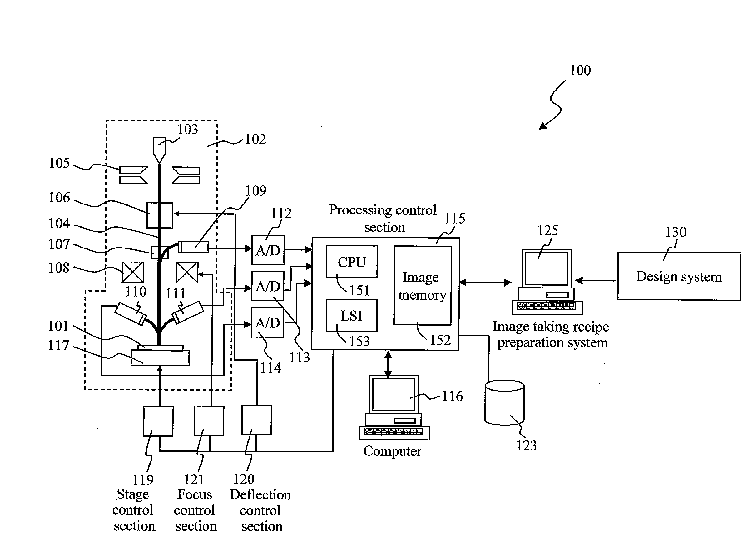
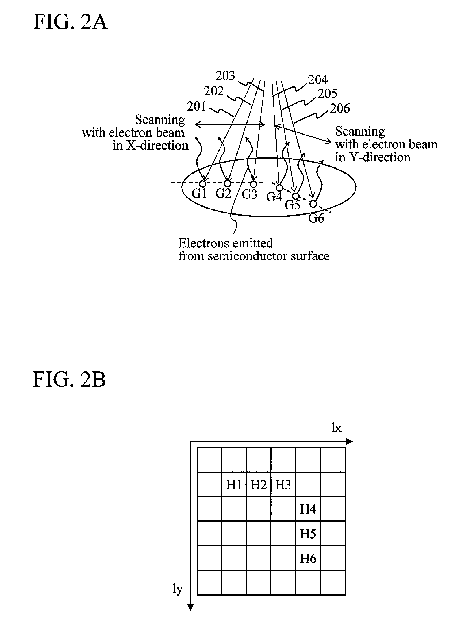
[0092]FIG. 1 is a diagram schematically showing the configuration of a pattern inspection system 1 in accordance with the present invention. The pattern inspection system 100 is provided with a scanning electron microscope (SEM) capable of obtaining a backscattered electron (BSE) image and a secondary electron (SE) image of a semiconductor pattern. An electron optical system 102 of the SEM has an electron gun 103 which produces an electron beam (primary electrons) 104, a condenser lens 105 which converges the electron beam 104 generated from the electron gun 103, a deflector 106 which deflects the converged electron beam 104, an E×B deflector 107 for detecting secondary electrons, and an objective lens 108 which focuses the converged electron beam on a semiconductor wafer 101. The semiconductor wafer 101 is placed on an XY stage 117. With the deflector 106 and the objective lens 108, the electron beam application positi...

second embodiment

(1) Pattern Inspection Processing

[0132]FIG. 21 is a flowchart for explaining pattern inspection processing according to a second embodiment of the present invention. Pattern inspection method according to the second embodiment is characterized in that an object from which a contour line to be used for comparison with design data is to be extracted can be selected from BSE images and an SE image.

[0133]A BSE image can be said to be an image suitable for contour line extraction because it is not easily affected by electrification in comparison with an SE image. In some case, however, an SE image can be obtained as an image more advantageous in contour line extraction, depending on SEM observation conditions, and wafer conditions including the wafer material and a manufacturing step condition. For example, in a case where pattern inspection is performed by taking BSE images in a high-pattern-density area at a low magnification as shown in FIG. 22A, there is a possibility of each of patt...


PUM


Abstract

A pattern data examination method and system capable of accurately and speedily examining a circuit pattern without failing to extract pattern contour data are provided. While pattern comparison is ordinarily made by using a secondary electron image, a contour of a pattern element is extracted by using a backscattered electron image said to be suitable for observation and examination of a three dimensional configuration of a pattern element, and pattern inspection is executed by using the extracted contour of the pattern element. More specifically, pattern inspection is executed by comparing a contour of a pattern element with design data such as CAD data to measure a difference between the contour and the data, and by computing, for example, the size of the circuit pattern element from the contour of a pattern. From two or more backscattered electron images formed by detecting backscattered electrons at two or more different spatial positions, pattern contour data contained in the backscattered electron images may be obtained.

Description

BACKGROUND OF THE INVENTION[0001]1. Field of the Invention[0002]The present invention relates to a pattern inspection method and a pattern inspection system and, more particularly, to a pattern inspection method and a pattern inspection system for examining a pattern formed on a substrate by using a photographic image of a semiconductor circuit and design data of the semiconductor circuit.[0003]2. Background Art[0004]In recent years, the development of semiconductor devices manufactured by finer patterning, having increased numbers of layers in multiplayer structure and complicated in logic has been pursued. In the present circumstances, it is extremely difficult to manufacture such semiconductor devices. As a result, the occurrence of defects coming from manufacturing processes tends to increase, and it is important to efficiently and correctly detect such defects and to identify manufacturing process problems.[0005]The kinds of possible defects from a manufacturing process include...

Claims


Application Information

Patent Timeline
IPC IPC(8): G01N23/00G01N23/225G03F1/84G03F1/86H01J37/22H01J37/244H01L21/027H01L21/66
CPCH01L22/12H01L2924/0002H01L2924/00
Inventor TOYODA, YASUTAKASOUDA, YASUNARITAKAGI, YUJIARAI, KOJI
Owner HITACHI HIGH-TECH CORP
Why Eureka
Try Eureka