Chip Resistor and Its Manufacturing Method

Active Publication Date: 2009-02-12
ROHM CO LTD
View PDF8 Cites 6 Cited by
  • Summary
  • Abstract
  • Description
  • Claims
  • Application Information

AI Technical Summary

Benefits of technology

[0024]According to the present invention, defective soldering due to the thermal expansion or contraction of the insulating substrate is reduced, and the current flow path can be

Problems solved by technology

With a short current flow path, breakage or deterioration of the chip resistor is likely to occur due to the application of instantaneous high voltage or surge voltage, and in this sense the arrangement of th

Method used


Image

  • Chip Resistor and Its Manufacturing Method
  • Chip Resistor and Its Manufacturing Method
  • Chip Resistor and Its Manufacturing Method

Examples


Example

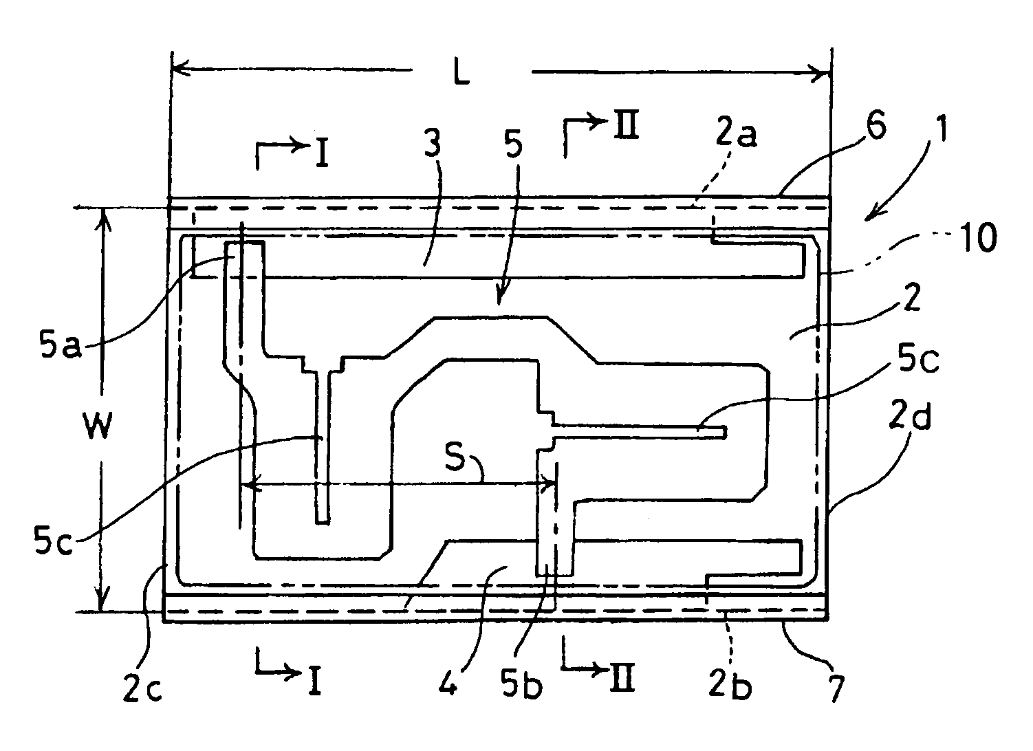
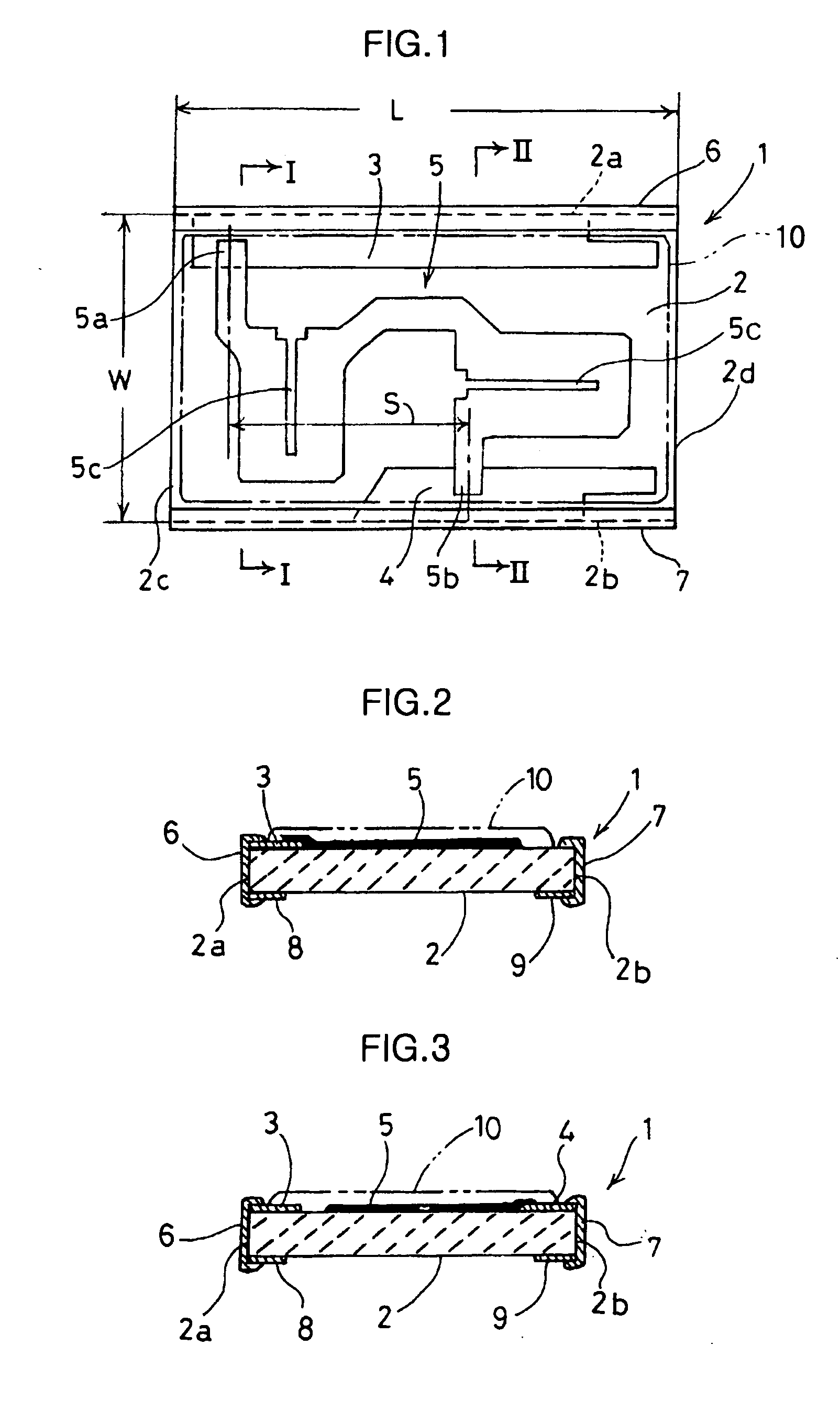
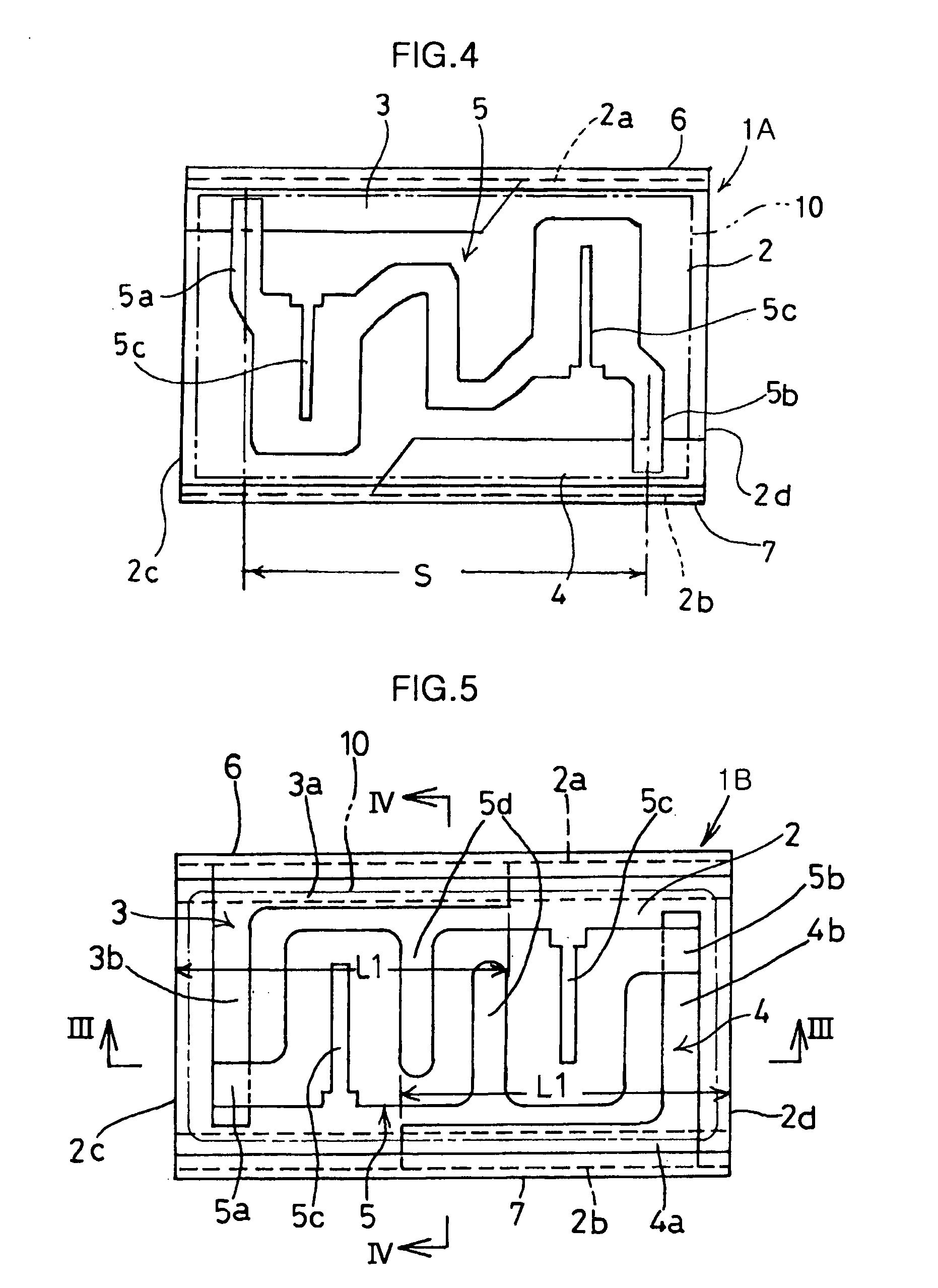
[0042]FIGS. 1-3 show a chip resistor according to a first embodiment of the present invention.

[0043]The chip resistor 1 according to the first embodiment at least includes an insulating substrate 2, a pair of upper electrodes 3 and 4, a resistor film 5, a pair of terminal electrodes 6 and 7, a pair of lower electrodes 8 and 9 and a cover coat 10.

[0044]The insulating substrate 2 is made of a heat-resistant insulating material such as a ceramic material and in the form of a chip having an elongated rectangular shape with a longer side L and a shorter side W. The upper electrode 3 is in the form of a strip formed on the upper surface of the insulating substrate 2 at a portion adjacent to a longer side surface 2a to extend along the longer side surface 2a. The upper electrode 4 is in the form of a strip formed on the upper surface of the insulating substrate 2 at a portion adjacent to a longer side surface 2b to extend along the longer side surface 2b. The resistor film 5 is formed betw...

Example

[0058]Referring to FIG. 4, a chip resistor 1A according to a second embodiment of the present invention will be described.

[0059]The chip resistor 1A shown in FIG. 4 has a configuration different from that of FIG. 1 in that the second U-shaped resistor portion connected to the connection portion 5b is oriented in the direction perpendicular to the longitudinal direction of the insulating substrate 2, and in that the two U-shaped resistor portions are connected to each other via an S-shaped resistor portion. This structure may compare with a structure obtained by turning the U-shaped resistor portion connected to the connection portion 5b of FIG. 1 counterclockwise by 90 degrees.

[0060]In the chip resistor 1A of the second embodiment, the position at which the connection portion 5b is connected to the upper electrode 4 is closer to the end surface 2d than in the chip resistor 1 of the first embodiment. Thus, the distance S between the two connection portions 5a and 5b, and hence the le...

Example

[0061]FIGS. 5-7 show a chip resistor 1B according to a third embodiment of the present invention.

[0062]The chip resistor 1B differs from the chip resistor 1 of the first embodiment in shape of the upper electrodes 3, 4 and resistor film 5 and the connection between the upper electrodes 3, 4 and the resistor film 5.

[0063]The upper electrodes 3 and 4 are L-shaped as viewed in plan. The upper electrode 3 includes a first portion 3a which is in the form of a strip formed on the upper surface of the insulating substrate 2 at a portion adjacent to the longer side surface 2a to extend along the longer side surface 2a. The upper electrode 3 further includes a second portion 3b which is in the form of a strip formed on the upper surface of the insulating substrate 2 at a portion adjacent to the short end surface 2c to extend along the short end surface 2c. The upper electrode 4 includes a first portion 4a which is in the form of a strip formed on the upper surface of the insulating substrate...


PUM

PropertyMeasurementUnit
Lengthaaaaaaaaaa
Distanceaaaaaaaaaa

Abstract

A chip resistor (1) according to the present invention includes an insulating substrate (2) which is in the form of an elongated rectangle in plan view, a pair of upper electrodes (3, 4) in the form of a strip formed on the upper surface of the insulating substrate (2) at portions adjacent to the long side surfaces of the insulating substrate to extend along the side surfaces, a resistor film (5) formed on the upper surface of the insulating substrate (2) and electrically connected to the upper electrodes (3, 4), and a pair of terminal electrodes (6, 7) formed on the two long side surfaces of the insulating substrate and electrically connected to the upper electrodes (3, 4), respectively. One of two longitudinal ends of the resistor film (5) is connected to one of the upper electrodes (3), whereas the other one of the two longitudinal ends of the resistor film is connected to the other one of the upper electrodes (4). The connection position at which the resistor film (5) is connected to the one of the upper electrodes (3) and the connection position at which the resistor film (5) is connected to the other one of the upper electrodes (4) are spaced from each other by a predetermined distance in the longitudinal direction of the upper surface of the insulating substrate (2).

Description

TECHNICAL FIELD[0001]The present invention relates to a chip resistor having high surge resistance, and also to a method for manufacturing such a chip resistor.BACKGROUND ART[0002]Chip resistors in general include an insulating substrate and terminal electrodes for soldering, where the substrate appears to be an elongated rectangle as viewed in plan, and each of the terminal electrodes is formed on one of the two end surfaces adjacent to the shorter sides of the elongated rectangle.[0003]FIG. 15 is a perspective view showing a typical chip resistor. The chip resistor 101 includes an insulating substrate 102 whose upper surface is formed with upper electrodes 103 and 104 disposed at the ends of the upper surface spaced from each other in the longitudinal direction of the substrate. The upper surface of the substrate 102 is also formed with a resistor film 105 extending in the longitudinal direction of the insulating substrate 102. The ends of the resistor film 105 overlap the upper e...

Claims


Application Information

Patent Timeline
IPC IPC(8): H01C1/142H01C1/012H01C17/06
CPCH01C1/012Y10T29/49099H01C17/006H01C1/142
Inventor YONEDA, MASAKI
Owner ROHM CO LTD
Why Eureka
Try Eureka