Built-in redundancy analyzer and method for redundancy analysis

a redundancy analysis and analyzer technology, applied in the field of built-in redundancy analyzers, can solve the problems of increasing the complexity of the circuit layout, occupying a lot of chip space, and not being realistic, and achieve the effect of reducing the analysis time and chip space used of flexibly analyzing different sizes and redundancy structures

Inactive Publication Date: 2009-02-19
FARADAY TECH CORP
View PDF14 Cites 4 Cited by
  • Summary
  • Abstract
  • Description
  • Claims
  • Application Information

AI Technical Summary

Benefits of technology

[0013]According to the BIRA and the redundancy analysis method provided by the present invention, a fault location information output by a built-in tester is converted into a general format according to a parameter of a fault memory and is then analyzed, and an analysis result is then converted into the format of the fault memory according to the parameter and is output to the fault memory. Accordingly, a plurality of memories having different sizes and redundancy structures can be analyzed flexibly. Moreover, an optimal design of the BIRA in the present invention can be provided regarding a plurality of repairable memories, so that the analysis time and chip space used thereof can be both reduced.

Problems solved by technology

It may be a big problem for testing a chip when the circuit on the chip includes a plurality of memories.
Such a large quantity of wirings takes up a lot of chip space and increases the complexity of the circuit layout, and moreover, is not realistic when the pin number of the chip is limited.
Multiple built-in redundancy analyzers are required correspondingly if the circuit on a chip includes a plurality of memories, which not only takes up a lot of chip space but also increases the cost of the chip.
The circuit illustrated in FIG. 1 becomes unrealistic when the number of built-in redundancy analyzers increases along with the increase of the number of memories.
However, the processor takes longer time for testing and analyzing the memories and takes up more chip space when compared with the circuit illustrated in FIG. 1.

Method used


Image

  • Built-in redundancy analyzer and method for redundancy analysis
  • Built-in redundancy analyzer and method for redundancy analysis
  • Built-in redundancy analyzer and method for redundancy analysis

Examples


Embodiment Construction

[0023]Reference will now be made in detail to the present preferred embodiments of the invention, examples of which are illustrated in the accompanying drawings. Wherever possible, the same reference numbers are used in the drawings and the description to refer to the same or like parts.

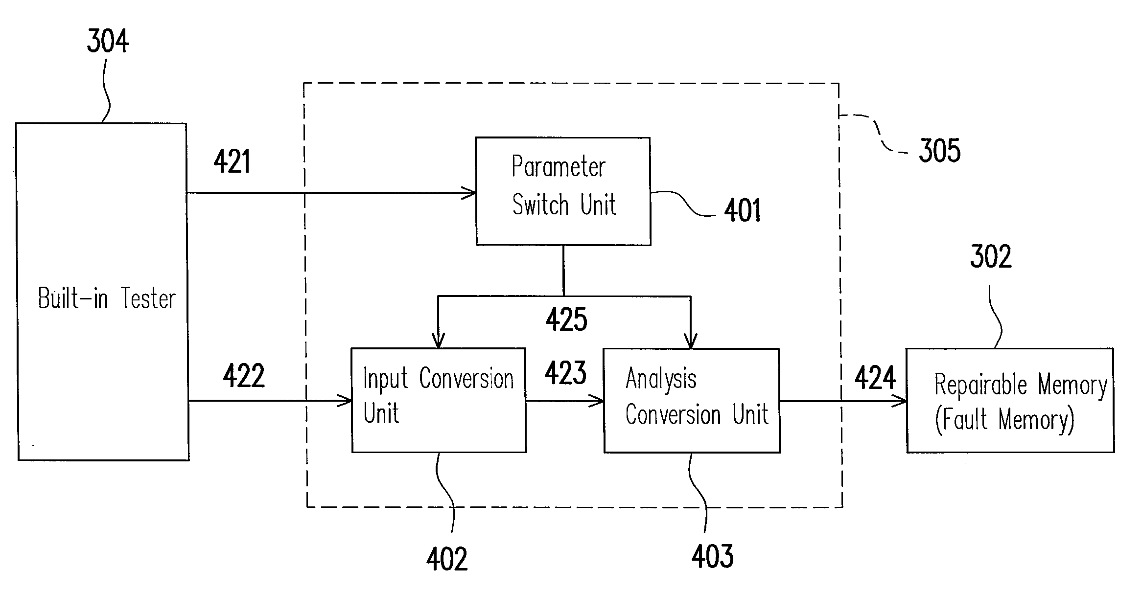
[0024]FIG. 3 is a diagram of a built-in self repair (BISR) circuit according to an embodiment of the present invention. Referring to FIG. 3, the BISR circuit is fabricated in a single chip and includes, demonstratively, three repairable memories 301˜303. However, the BISR circuit may include any number of repairable memories according to the present invention. A built-in tester 304 tests the repairable memories 301˜303 and notifies a fault to the built-in redundancy analyzer (BIRA) 305. The BIRA 305 performs a redundancy repair analysis according to a fault information received from the built-in tester 304 and then provides an analysis result to the repairable memory containing the fault (referred as...


PUM


Abstract

A built-in redundancy analyzer and a redundancy analysis method thereof for a chip having a plurality of repairable memories are provided. The method includes the following steps. First, the identification code of a repairable memory containing a fault (“fault memory” for short) is identified and a parameter is provided according to the identification code. The parameter includes the length of row address, the length of column address, the length of word, the number of redundancy rows, and the number of redundancy columns of the fault memory. Since the parameter of every individual repairable memory is different, the fault location is converted into a general format according to the parameter for easier processing. A redundancy analysis is then performed according to the parameter and the converted fault location, and the analysis result is converted from the general format to the format of the fault memory and output to the fault memory.

Description

BACKGROUND OF THE INVENTION[0001]1. Field of the Invention[0002]The present invention generally relates to a built-in self repair (BISR) technique of a memory, in particular, to a built-in redundancy analyzer (BIRA) and a redundancy analysis method thereof.[0003]2. Description of Related Art[0004]It may be a big problem for testing a chip when the circuit on the chip includes a plurality of memories. The input and output terminals of all the memories have to be connected to outside of the chip if an external apparatus is used for testing the chip. Such a large quantity of wirings takes up a lot of chip space and increases the complexity of the circuit layout, and moreover, is not realistic when the pin number of the chip is limited. Accordingly, a concept of built-in self test (BIST) is provided. BIST is to build a testing circuit and the memories to be tested on the same chip, so that the input and output terminals of the memories do not have to be connected to outside of the chip ...

Claims


Application Information

Patent Timeline
Patent Type & Authority Applications(United States)
IPC IPC(8): G06F11/22
CPCG11C29/16G11C29/44G11C2029/0401G11C29/70G11C29/4401
Inventor TSENG, TSU-WEIHSU, CHIH-CHIANGLI, JIN-FUPAO, CHIEN-YUAN
Owner FARADAY TECH CORP
Why Eureka
Try Eureka