

Apparatus for cleaning substrate and method for cleaning substrate
a technology for cleaning apparatus and substrates, applied in the direction of cleaning process and apparatus, cleaning apparatus and process, chemistry apparatus and process, etc., can solve the problems of difficult to remove small impurity particles from substrates using typical substrate cleaning methods, the need for impurity removal process, and the small allowable impurity particle size of substrates, etc., to achieve efficient apparatus and method for cleaning substrates
- Summary
- Abstract
- Description
- Claims
- Application Information
AI Technical Summary
Benefits of technology
Problems solved by technology
Method used
Image

Examples
Embodiment Construction
[0017]Preferred embodiments of the present invention will be described below in more detail with reference to the accompanying drawings. The present invention may, however, be embodied in different forms and should not be construed as limited to the embodiments set forth herein. Rather, these embodiments are provided so that this disclosure will be thorough and complete, and will fully convey the scope of the present invention to those skilled in the art.
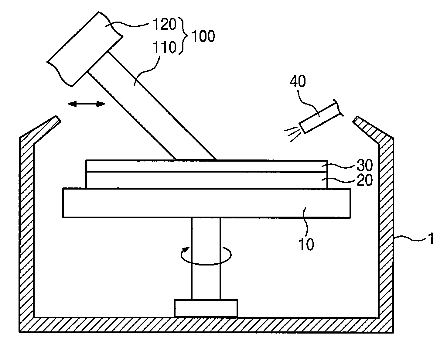
[0018]FIG. 1 is a schematic cross-sectional view illustrating an apparatus for cleaning a substrate according to an embodiment of the present invention;
[0019]Referring to FIG. 1, the substrate cleaning apparatus includes a cleaning container 1, a stage 10, a cleaning liquid supply unit 40, and a vibration unit 100. The stage 10 is mounted on the bottom of the cleaning container 1. A substrate 20 is placed on the stage 10. The stage 10 may be a chuck configured to support and fix the substrate 20. The chuck may fix the substrate 20 u...
PUM
 Abstract
Description
Claims
Application Information