Method and device for reducing voltage stress at bootstrap point in electronic circuits

a technology of electronic circuits and bootstrap points, applied in the field of electronic circuits, can solve the problems of unnecessarily high voltage differential across the first transistor, imposing etc., and achieve the effect of reducing the voltage differential and reducing the stress on the first transistor

Active Publication Date: 2009-02-26
AU OPTRONICS CORP
View PDF7 Cites 37 Cited by
  • Summary
  • Abstract
  • Description
  • Claims
  • Application Information

AI Technical Summary

Benefits of technology

[0011]In a shift register module having a plurality of shift register units arranged in a cascade fashion, the shift register unit at a current stage receives an output pulse from the shift register unit at the previous stage to produce an output pulse of the current stage. Typically, a first transistor is coupled to the output of the previous stage shift register unit and used as a switch to receive the output pulse from the previous stage. At the arrival of the previous stage output pulse, the transistor is operated in a conducting state. The previous stage output pulse is conveyed to a gate terminal of a second transistor in the current shift register unit for causing the second transistor to be in a conducting state. After receiving that output pulse, the first transistor is operated in a non-conducting state and an output pulse is produced in the current stage shift register unit. While the current stage shift register unit outputs an output pulse, the voltage differential across the first transistor is unnecessarily high, imposing a stress on the first transistor. The present invention provides a method and a circuit element for reducing the stress on the first transistor in the period when the current stage shift register unit outputs its output pulse. In particular, the present invention uses a discharging circuit coupled to the gate terminal of the second transistor to reduce the voltage differential across the first transistor.

Problems solved by technology

While the current stage shift register unit outputs an output pulse, the voltage differential across the first transistor is unnecessarily high, imposing a stress on the first transistor.

Method used


Image

  • Method and device for reducing voltage stress at bootstrap point in electronic circuits
  • Method and device for reducing voltage stress at bootstrap point in electronic circuits
  • Method and device for reducing voltage stress at bootstrap point in electronic circuits

Examples


Embodiment Construction

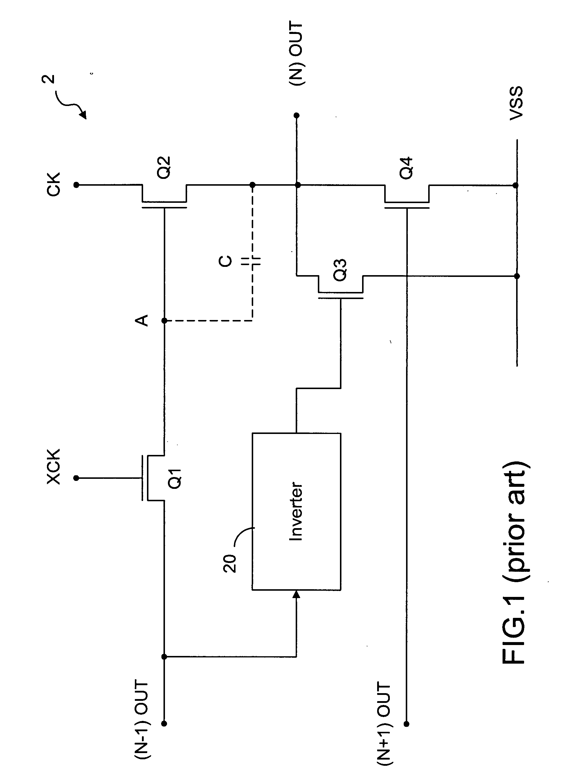
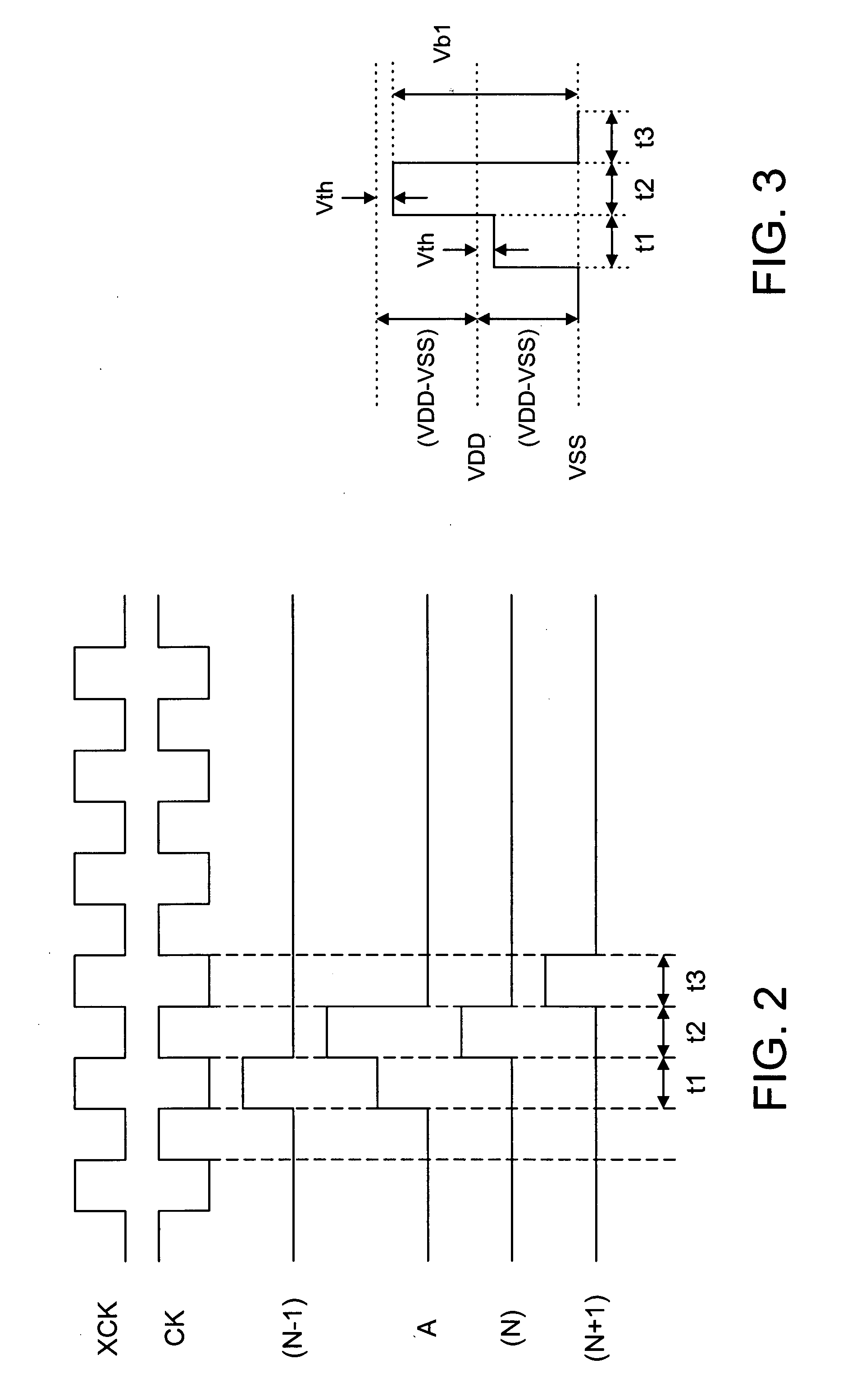
[0125]The objective of the present invention is to reduce the voltage level at a bootstrap point, so as to reduce the voltage stress imposed on the transistor or transistors coupled to the bootstrap point. The bootstrap point exists in a circuit where a first transistor is used as a switch to provide a bias voltage level to the gate of a second transistor at a clock cycle and to maintain the charge at that gate at a complementary clock cycle. The bootstrap point is located at the gate of the second transistor. If the voltage level at the bootstrap point gives rise to a relative high source-drain voltage of the first transistor at the complementary clock cycle, this source-drain voltage imposes a high stress on the first transistor. A bootstrap circuit section is shown in FIG. 9.

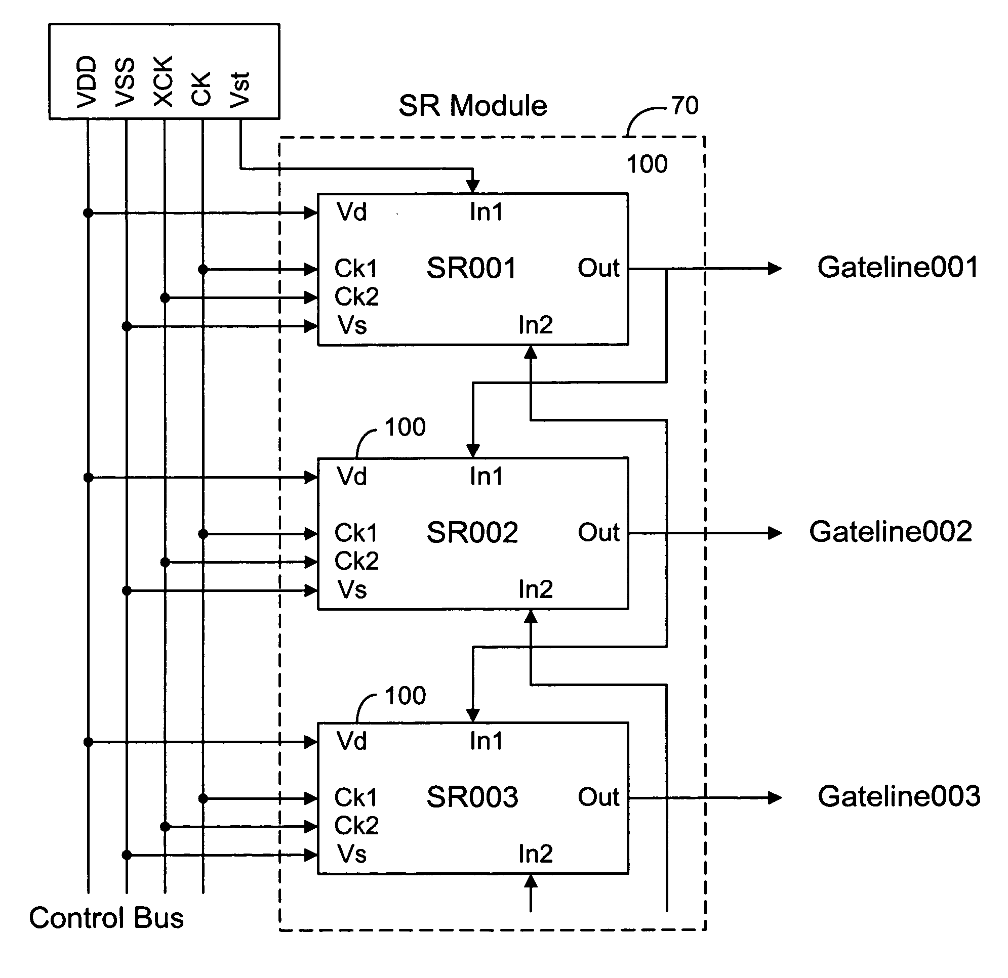
[0126]In this disclosure, a shift register circuit is used to show the bootstrap point in the circuit and to illustrate how the voltage level at the bootstrap point is resulted. In the shift register circuit ...


PUM


Abstract

A discharging device is used to reduce the voltage level at a bootstrap point in an electronic circuit such as a shift register circuit. In such a circuit, a first transistor in a conducting state receives an input pulse and conveys it to the gate terminal of a second transistor, causing the second transistor to be in a conducting state. This gate terminal is known as a bootstrap point. After receiving the input pulse, an output pulse is produced at one drain/source terminal of the second transistor. During the time period of the output pulse, the first transistor is in a non-conducting state and the voltage level at the bootstrap point is high, imposing a stress upon the first transistor. A discharging circuit consisting of at least one transistor is coupled to the bootstrap point in order to reduce the voltage level at the output pulse period.

Description

FIELD OF THE INVENTION [0001]The present invention relates to an electronic circuit, such as a shift register circuit and, more particularly, to an electronic circuit having a bootstrap point.BACKGROUND OF THE INVENTION [0002]Shift registers are commonly used to drive a display panel, such as a thin-film transistor liquid-crystal display (TFT-LCD) panel. In a typical TFT-LCD display panel, a plurality of pixels are arranged in a two-dimensional array. These pixels are controlled by a plurality of data lines and a plurality of gate lines. The data lines are connected to a data source driver and the gate lines are connected to a gate line driver. A gate line driver comprises a shift register module having a plurality of shift register units connected in a cascade manner such that the output of a shift register unit in a stage is connected to the input of a shift register unit of the subsequent stage. The output of each shift register unit in a shift register module is connected to a g...

Claims


Application Information

Patent Timeline
Patent Type & Authority Applications(United States)
IPC IPC(8): G09G3/36G11C19/00
CPCG09G3/3677G11C19/28G09G2330/04G09G2310/0286
Inventor LIU, SHENG-CHAOCHEN, CHEN-MINGLIN, MING-TIEN
Owner AU OPTRONICS CORP
Why Eureka
Try Eureka