Semiconductor storage device and method of controlling semiconductor storage device

a semiconductor storage device and storage device technology, applied in the direction of memory address/allocation/relocation, instruments, computing, etc., can solve the problems of inefficient parallel processing of the chips, etc., to prevent deterioration in write/read performance of the device, reduce the time each chip is in an idle state, and prevent performance deterioration

Active Publication Date: 2009-03-12
HITACHI LTD
View PDF11 Cites 102 Cited by
  • Summary
  • Abstract
  • Description
  • Claims
  • Application Information

AI Technical Summary

Benefits of technology

[0012]With the above configuration, in a semiconductor storage device configured to execute parallel processing to plural flash memory chips and that performs memory control to record update data by using blank pages in a physical block in each chip, memory command tasks to be subjected to parallel processing are uniformly distributed to the memory chips during data merge copy executed in the device when writing the data from the device, or during reading data to the device. This reduces the time each chip is in an idle state. Accordingly, the effect of preventing deterioration in write / read performance of the device can be obtained.
[0013]According to the invention, a semiconductor storage device that enables prevention of deterioration in performance and a method of controlling the semiconductor storage device can be provided.

Problems solved by technology

When a control method in which blank pages in a physical block are utilized to record update data, which is as shown in U.S. Pat. No. 7,039,788, is utilized in the semiconductor storage device provided with plural flash memory chips, and the chips are subjected to parallel processing to improve performance, which is as shown in JP2006-127234 A, the parallel processing involving the chips may be executed inefficiently, due to the recorded state of the update data, leading to deterioration in write / read performance.

Method used


Image

  • Semiconductor storage device and method of controlling semiconductor storage device
  • Semiconductor storage device and method of controlling semiconductor storage device
  • Semiconductor storage device and method of controlling semiconductor storage device

Examples


Embodiment Construction

[0033]An embodiment of the present invention will be described with reference to the accompanying drawings.

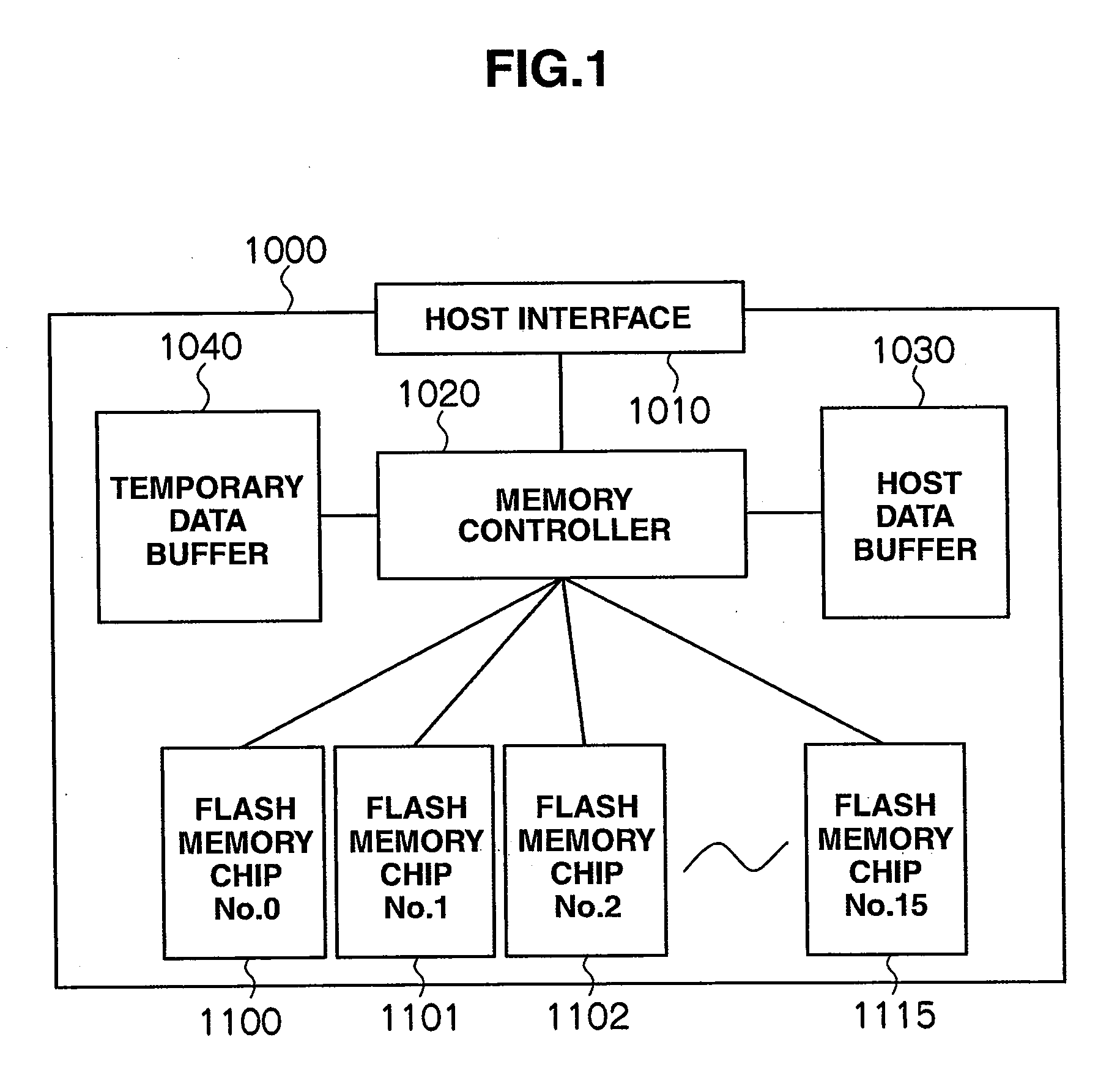
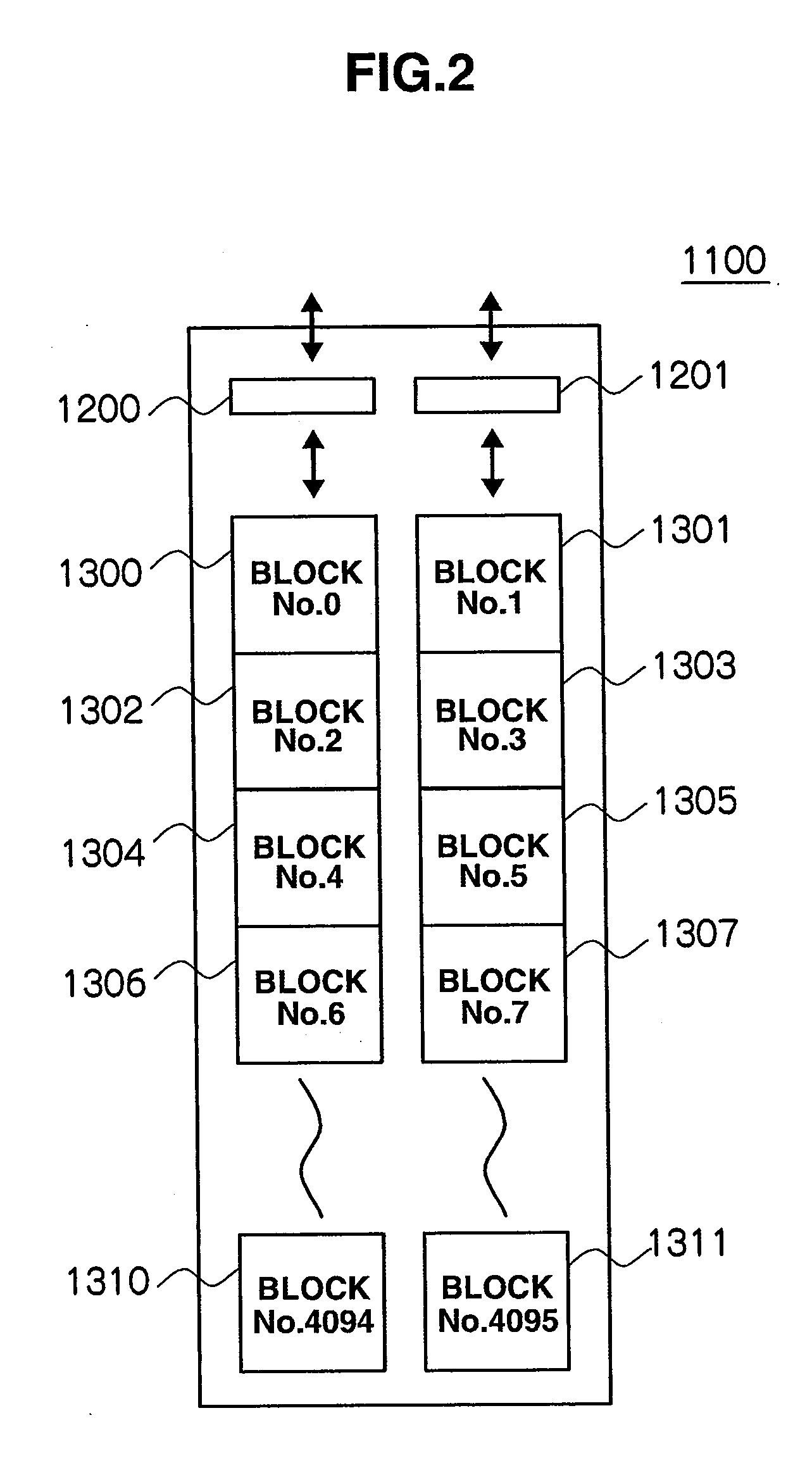
[0034]FIG. 1 is a diagram briefly showing an internal configuration for a semiconductor storage device 1000 that utilizes the invention. The semiconductor storage device 1000 is composed of a host interface 1010, a memory controller 1020, a host data buffer 1030, a temporary data buffer 1040, and plural (e.g., 16) flash memory chips 1100 to 1115.

[0035]The host interface 1010 is an interface mechanism connected to an external host(s) (not shown in the drawing), and transmits data stored in the flash memory chips 1100 to 1115 to the host and receives write data to be stored in the flash memory chips 1100 to 1115 from the host in response to read / write request commands from the host.

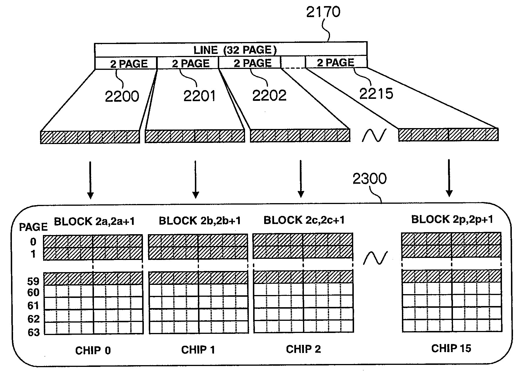
[0036]Incidentally, the host specifies a logical storage position for the data requested to be subject to read / write by using a logical address (hereinafter referred to as “LBA (Logical Block Address)”...


PUM


Abstract

In a semiconductor storage device, a memory controller divides each of blocks in each of chips into a first page set composed of pages and a second page set composed of pages, divides a logical address space into groups, and divides each group into lines. Block units are created each of which is obtained by assembling a predetermined number of blocks from the blocks in each chip. A predetermined number of block units from the block units are managed as standard block units, and the other block units are managed as spare block units. Each standard block unit is made to correspond to one group. The corresponding group data is stored in the pages in the first page set in each block constituting the standard block unit, and unwritten pages for recording update data for the group data are provided to be included in the second page set.

Description

CROSS-REFERENCES TO RELATED APPLICATIONS[0001]This application relates to and claims priority from Japanese Patent Application No. 2007-231640, filed on Sep. 6, 2007, the entire disclosure of which is incorporated herein by reference.BACKGROUND[0002]1. Field of the Invention[0003]The invention relates to a semiconductor storage device and a method of controlling the semiconductor storage device, and is particularly suitable for use in a semiconductor storage device using an electrically rewritable non-volatile memory as a storage medium and a method of controlling the semiconductor storage device.[0004]2. Description of Related Art[0005]A semiconductor storage device in which data in a logical block is distributed to plural flash memory physical blocks to be stored, and when the data stored in each of the physical blocks is updated, the relevant update data is recorded in a blank page in the physical block, and the original stored data is invalidated; and in which, if the physical b...

Claims


Application Information

Patent Timeline
Patent Type & Authority Applications(United States)
IPC IPC(8): G06F12/02
CPCG06F2212/7208G06F12/0246
Inventor MIZUSHIMA, NAGAMASA
Owner HITACHI LTD
Why Eureka
Try Eureka