Magneto-resistive effect device of the cpp structure and magnetic disk system
- Summary
- Abstract
- Description
- Claims
- Application Information
AI Technical Summary
Benefits of technology
Problems solved by technology
Method used
Image
Examples
experimental examples
[0143]The invention is now explained in further details with reference to some specific examples of the inventive magneto-resistive effect device.
experimental example 1
[0144]Experimentation was carried out to learn what influences the angle θ of magnetization of the inclined magnetization structure formed at the upper shield layer and the thickness h (see FIG. 3) of the upper shield layer had on the bias magnetic field generated (leaking) from the upper shield layer.
[0145]The angle θ of magnetization was changed to 5°, 10°, 15°, 20°, 25°, 30°, 35°, 40°, 45°, 55°, 70°, and 90°, respectively, and the thickness h of the upper shield layer was changed to 5 nm, 100 nm, and 200 nm, respectively.
[0146]The results are plotted in the graph of FIG. 13 with the angle θ of magnetization as abscissa and the bias magnetic field leaking from the upper shield layer as ordinate. The parameter is the thickness h of the upper shield layer. It is seen that as the angle θ of magnetization increases, so does the bias magnetic field. It is seen that when the angle θ of magnetization is 45°, a bias magnetic field of about 600 Oe is applied, and that even at an angle θ of...
experimental example 2
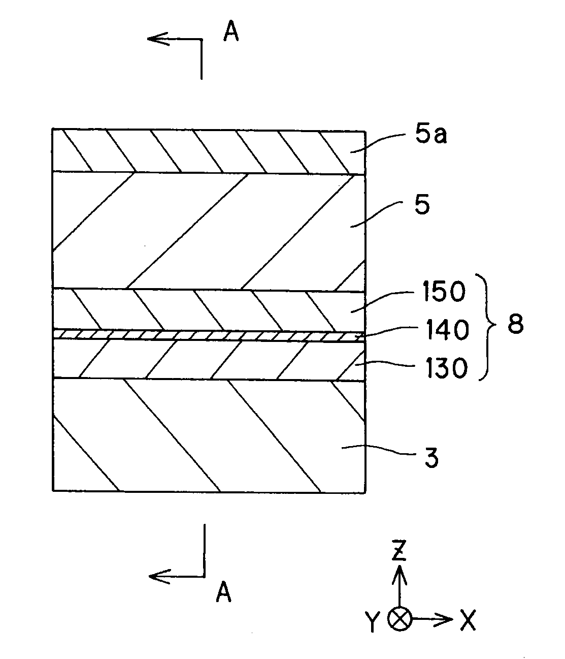
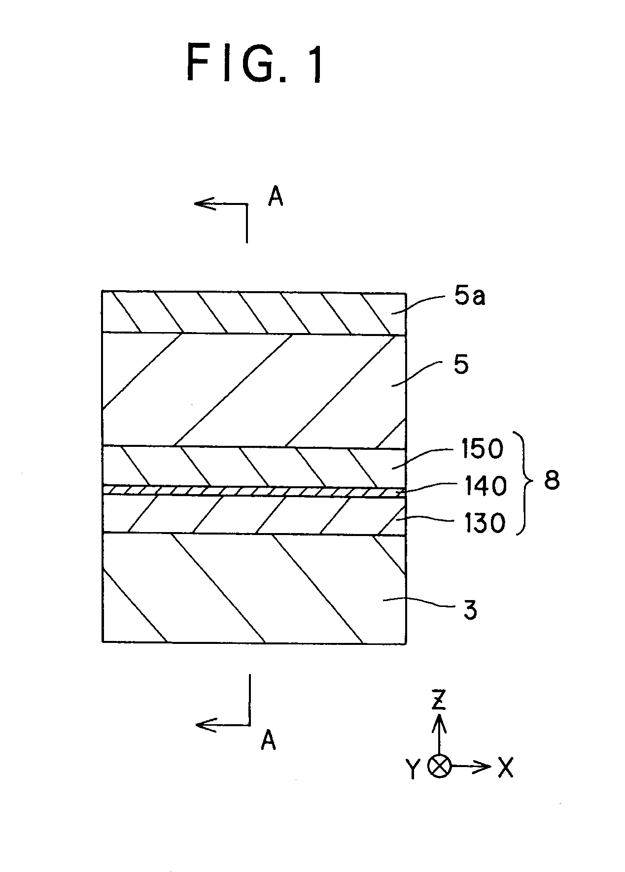
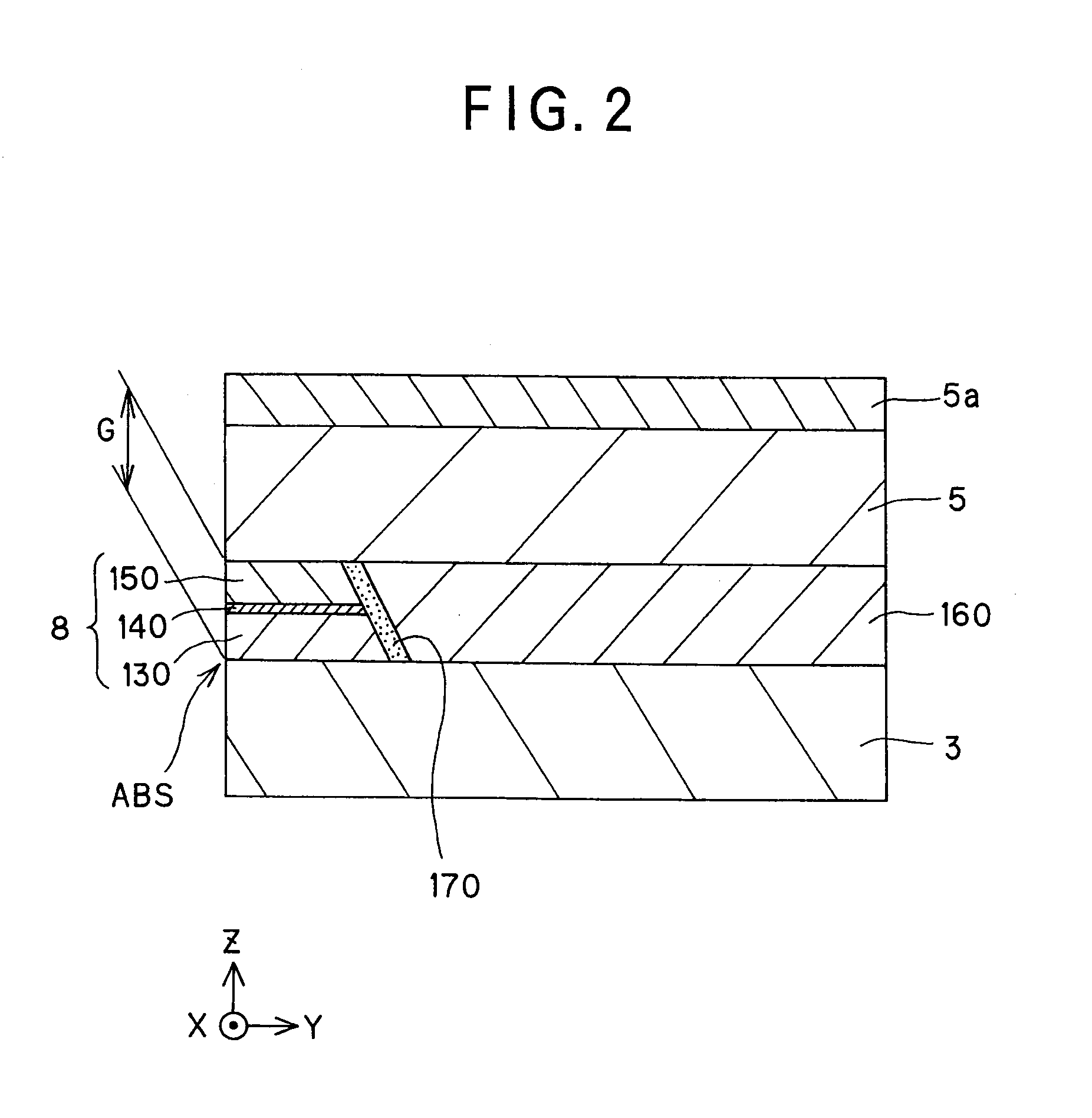
[0148]As shown in Table 1, the magneto-resistive effect unit 8 was formed on the lower shield layer 3 made of a 100-nm thick NiFe, the upper shield layer 5 made of a 100-nm thick NiFe was formed on that magneto-resistive effect unit 8, and the antiferromagnetic member 5a made of IrMn was formed on that upper shield layer 5.
[0149]The magneto-resistive effect device 8 was formed such that the first ferromagnetic layer 130 made of a 5-nm thick CoFe and the second ferromagnetic layer 150 made of a 5-nm thick CoFe were exchange coupled to each other via the nonmagnetic metal intermediate layer 140 made of a 1.0-nm thick Cu.
[0150]By exchange coupling with the antiferromagnetic member 5a made of IrMn, the upper shield layer 5 had its angle θ of magnetization set at 45°.
[0151]As a result of using such a magnetic field sensor to detect signal magnetic fields from the medium corresponding to −400 Oe to 400 Oe, it was found that there can be a practically available magnetic resistance change o...
PUM
 Abstract
Description
Claims
Application Information


