

Semiconductor device having decreased contact resistance
- Summary
- Abstract
- Description
- Claims
- Application Information
AI Technical Summary
Benefits of technology
Problems solved by technology
Method used
Image

Examples
first embodiment
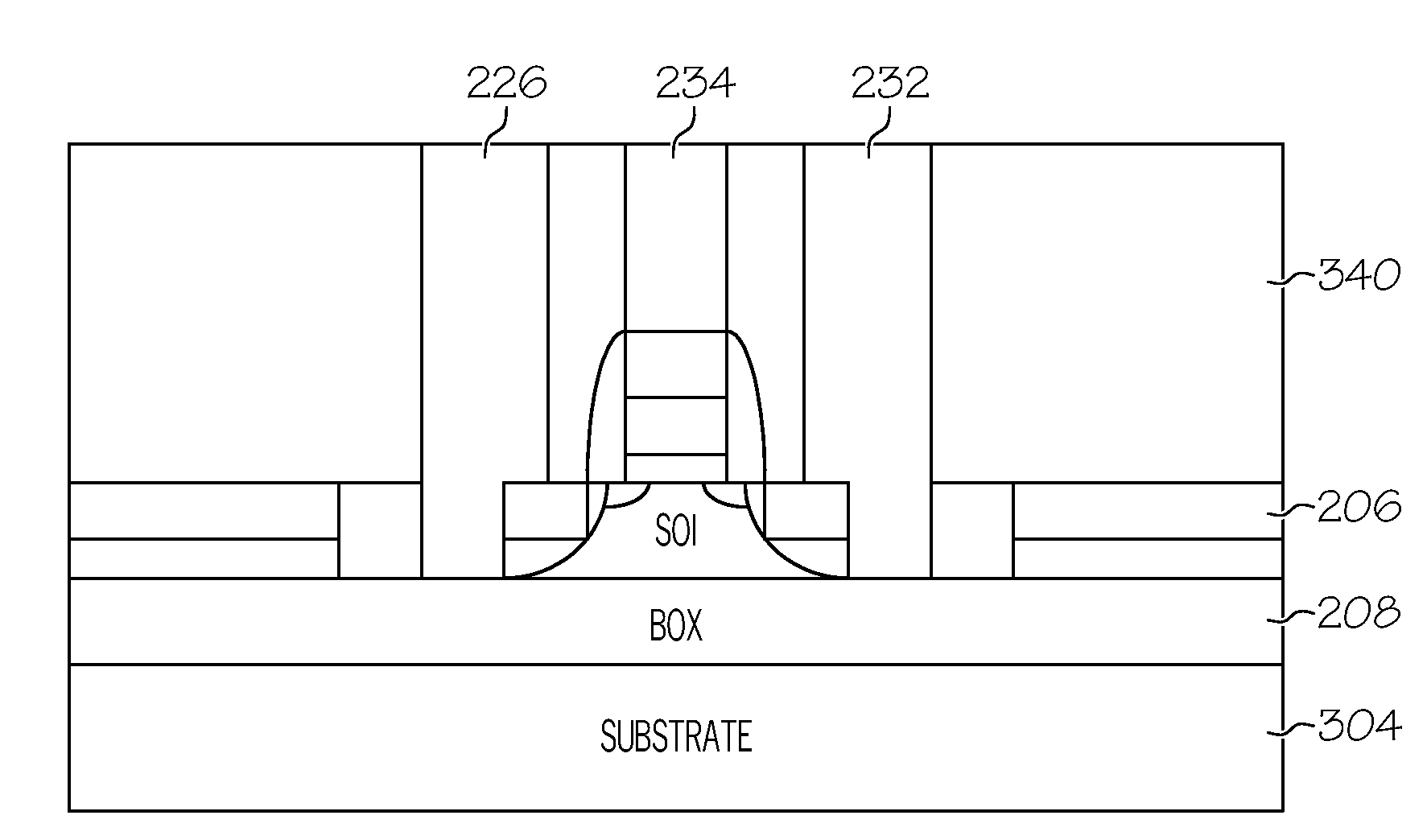
[0023]The second silicide region 212 has both a surface portion 222 and a sidewall portion 224 for physically and electrically connecting to contact 226. In a similar manner, the third silicide region 214 has both a surface portion 228 and a sidewall portion 230 for physically and electrically connecting to contact 232. Thus, the contacts 226, 232 are formed through the ILD layer (not shown) in accordance with this first embodiment such that they are physically connected to the silicide regions 212, 214 at both the surface portions 222, 228 and the sidewall portions 224, 230 to provide an electrical coupling through the ILD layer to the drain region 216 and the source region 218. Another contact 234 is physically connected to the silicide region 210 to provide an electrical coupling to the gate 202 through the ILD layer.
[0024]As can clearly be seen in the cross-sectional view of FIG. 6, the physical and electrical connection of the contacts 226, 232 to the silicide regions 212, 214 ...
second embodiment
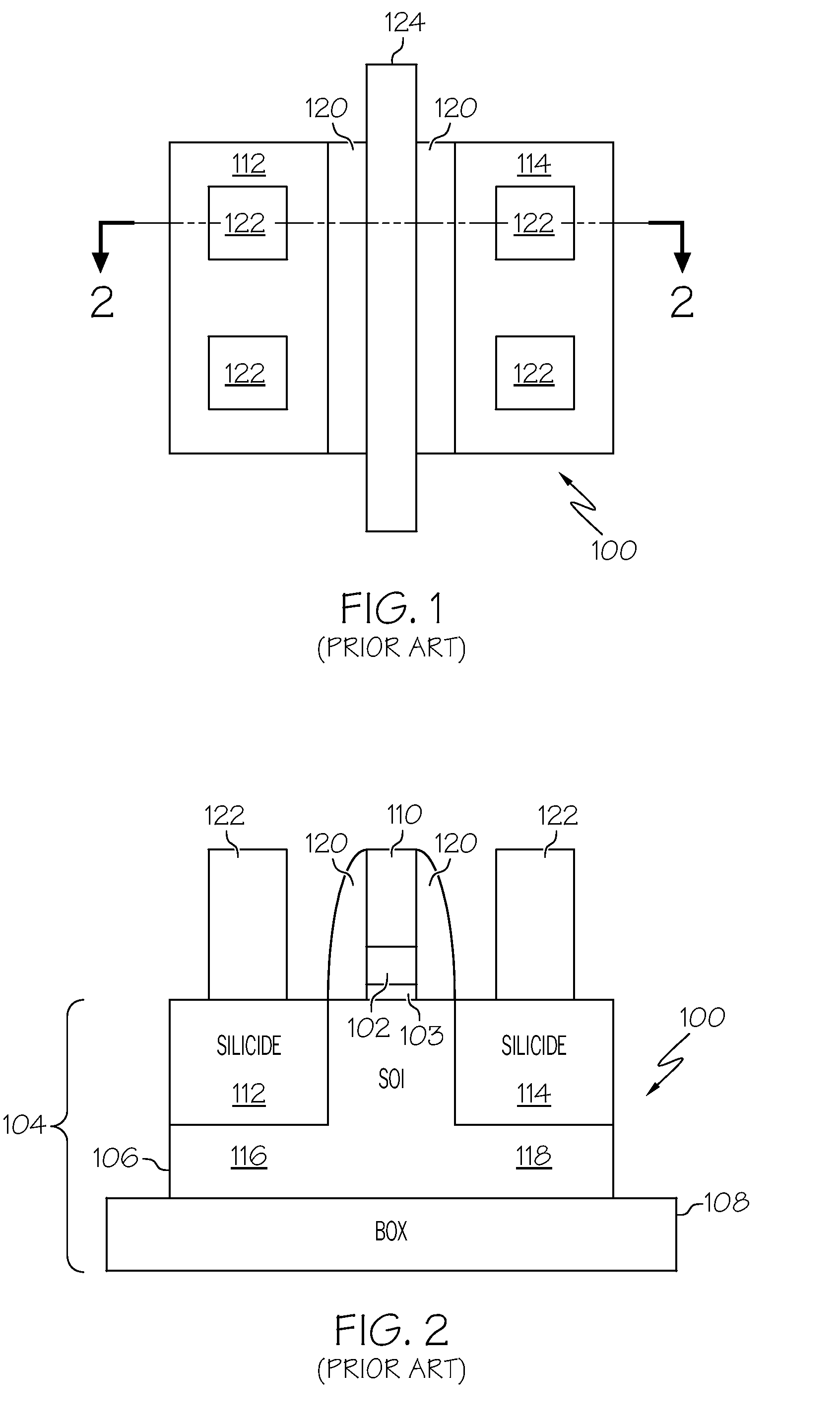
[0039]Multiple trenches have been etched in the silicide regions 410, 412 and the source region and the drain region 420 in a direction substantially perpendicular to the longitudinal axis 440 to expose multiple surface portions 450 and multiple sidewall portions 452 of the silicide regions 410, 412 and multiple sidewall portions 454 of the source region and the drain region 420 for physically and electrically connecting to contact fingers 455 of the contacts 430, 432. Thus, the contacts 430, 432 are formed through the ILD layer (not shown) in accordance with this second embodiment such that the contact fingers 455 physically and electrically connect to the silicide regions 410, 412 at multiple sidewall portions 452 and intermediate portions 457 of the contacts 430, 432 between the contact fingers 455 physically and electrically connect to the silicide regions 410, 412 at multiple surface portions 450 to provide an electrical coupling through the ILD layer to the source region and t...
PUM
 Abstract
Description
Claims
Application Information