
Method for processing an electroplated copper film in copper interconnect process

Active Publication Date: 2016-08-25
SHANGHAI INTEGRATED CIRCUIT RES & DEV CENT
View PDF1 Cites 1 Cited by
  • Summary
  • Abstract
  • Description
  • Claims
  • Application Information

AI Technical Summary

Benefits of technology

The present invention is about optimizing the copper back-end-of-line interconnect process in semiconductor device manufacturing. The first annealing process is performed at or below 180°C to avoid negative effects on device manufacturing caused by higher temperatures and the introduction of low dielectric constant intermetal dielectric materials. The anneal temperature is controlled to inhibit grain growth of the electroplated copper film and obtain fine grains which are beneficial in controlling dishing in the chemical mechanical polishing process. After the copper back-end-of-line interconnect process, a second annealing process is added at or beyond 240°C to induce recrystallization of copper to decrease the resistance of the electroplated copper film, improve contact resistance between the copper in the via and the copper in the underlying interconnects, further reduce RC time delay, and prevent negative effect on device manufacturing caused by high-temperature and short-time annealing processes. The invention is compatible with the standard copper / low-k back-end-of-line process integration.

Problems solved by technology

The RC time delay in the metal interconnect process has become a main part of the RC time delays in the whole chip manufacturing process.
Nowadays, the k value for the conventional ultra-low dielectric constant dielectric material has been reduced to about 2.0, however it still can't meet the requirement for further decreasing the metal line width.
The magnetron sputtering physical vapor deposition (PVD) is a conventional method for depositing the barrier layers and the seed layers, however which have limitation of step coverage.
However, the via resistance is still one of the critical factors for the RC time delay in copper interconnects.
The via etching process and cleaning process in the copper interconnect process could cause damages to surface of copper interconnects underlying the via; after the cleaning process, the surface of copper interconnects underlying the via exposes to the air, which will be oxidized; a barrier layer is deposited on the surface of copper interconnect underlying the via by a barrier layer deposition process; and the temperature for annealing the electroplated copper film is further decreased due to the introduction of ultra-low k dielectric materials.
Those would increase the contact resistance between the copper in the via and the copper in the underlying interconnects, which will result an increase in RC time delay.
However, the copper film in the via processed under this temperature is difficult to fully release impurities, thus, the structure with large grain size is difficult to form; even if the anneal duration is extended, the growth of the copper grain in the via is still limited, thus the resistance of the cooper film in the via is relatively high, and the contact resistance of the via is difficult to decrease.
Therefore, the conventional annealing process for the electroplated copper film limits the decrease of the contact resistance of the vias.

Method used


Image

  • Method for processing an electroplated copper film in copper interconnect process
  • Method for processing an electroplated copper film in copper interconnect process

Examples


Embodiment Construction

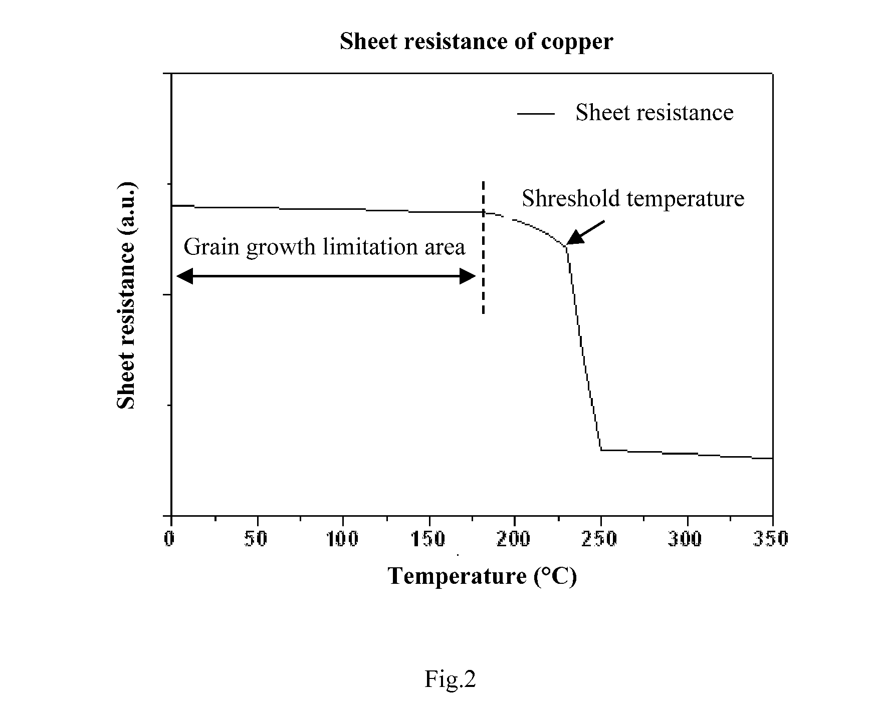
[0029]The present invention will now be descried more fully hereinafter with reference to the accompanying drawings. This invention may, however, be embodied in different forms and should not be construed as limited to the embodiments set forth herein. It will be understood by those skilled in the art that various changes in form and details may be made herein without departing from the spirit and scope of the invention.

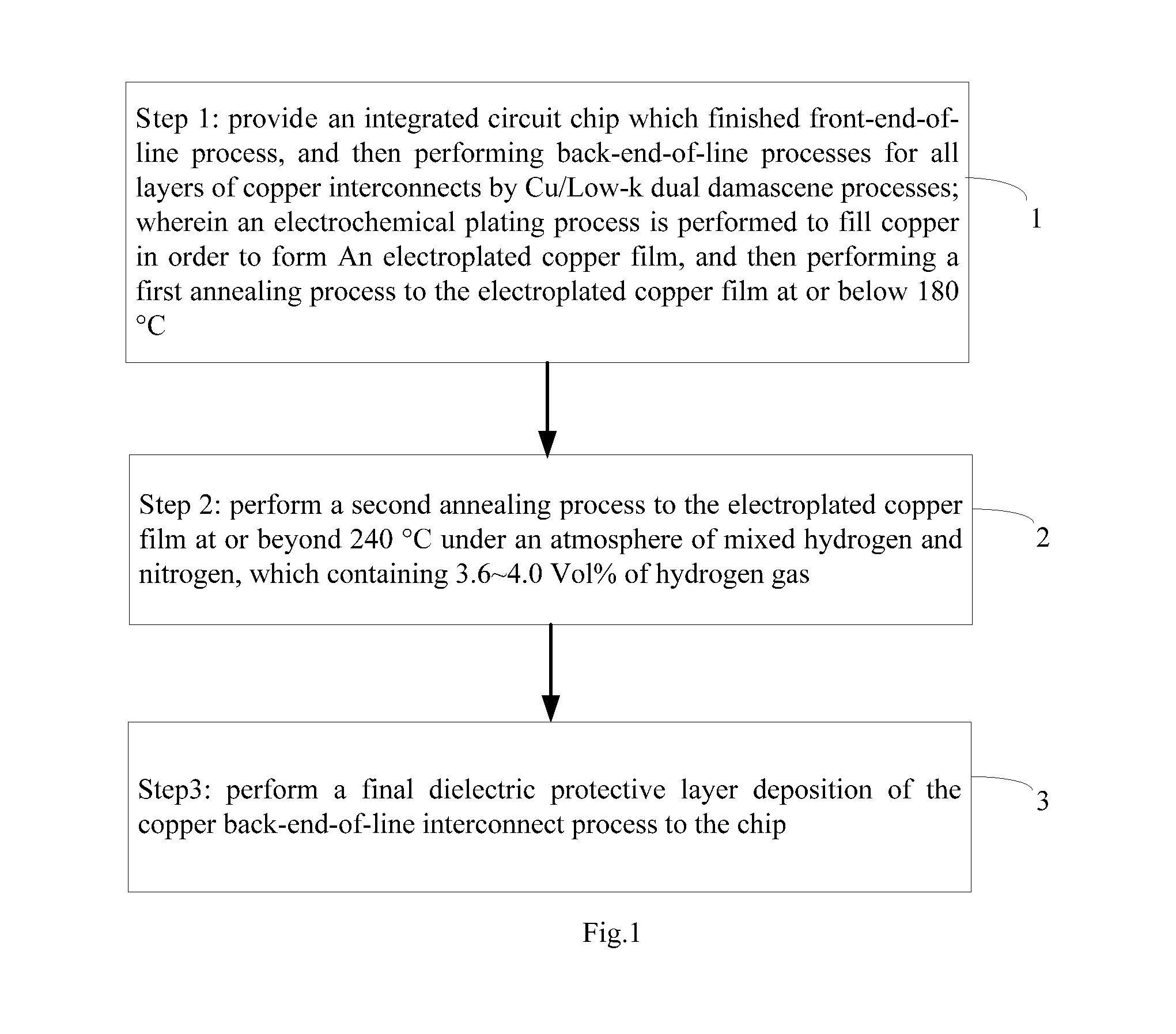
[0030]Referring to FIG. 1, illustrating a flow chart of the method for processing an electroplated copper film in copper interconnect process according to one embodiment of the present invention. In the embodiment, the method for processing the electroplated copper film includes the following steps:

[0031]As shown in the box 1 of the FIG. 1, the step 1 includes: providing an integrated circuit chip which finished front-end-of-line process, and then performing back-end-of-line processes for all layers of copper interconnects by Cu / Low-k dual damascene process; wherein ...


PUM


Abstract

A method for processing an electroplated copper film in copper interconnect process is disclosed by the present invention. Firstly, in the copper back-end-of-line interconnect process, the first annealing process for the electroplated copper film is performed at or below 180° C.; then, after the copper back-end-of-line interconnect process, another annealing process with higher temperature (equal or above 240° C.) to the electroplated copper film is performed to make the copper recrystallize, so as to decrease the resistivity of the electroplated copper film and form an interface state having lower resistivity at the interface of the vias bottom, which decrease the contact resistance between the vias and the underlying copper interconnects and further reduce the RC time delay in the vias. The present invention can be applied in the Cu / Low-k back-end-of-line interconnect process and compatible with the standard Cu / Low-k back-end-of-line process integration.

Description

CROSS-REFERENCE TO RELATED APPLICATION[0001]This application claims the priority benefit of International Patent Application Serial No. PCT / CN2014 / 085102, filed Aug. 25, 2014, which is related to and claims the priority benefit of China patent application serial No. 201410174828.9, filed Apr. 28, 2014. The entirety of each of the above-mentioned patent applications is hereby incorporated by reference herein and made a part of this specification.FIELD OF THE INVENTION[0002]The present invention generally relates to the field of semiconductor manufacturing, more particularly, to a method for processing an electroplated copper film in copper interconnect process which could decrease the contact resistance between the via and underlying metal and further reduce RC time delay.BACKGROUND OF THE INVENTION[0003]With the semiconductor manufacturing technology entering the sub-65nm technology node, the crosstalk or the electromagnetic interactions caused by proximity effects of various circui...

Claims


Application Information

Patent Timeline
IPC IPC(8): H01L21/768H01L21/02H01L21/321
CPCH01L21/288H01L21/768H01L21/02126H01L21/02167H01L21/76883H01L21/76802H01L21/7685H01L21/76879H01L21/3212H01L21/76838H01L2221/1068
Inventor LIN, HONG
Owner SHANGHAI INTEGRATED CIRCUIT RES & DEV CENT
Features
  • Generate Ideas
  • Intellectual Property
  • Life Sciences
  • Materials
  • Tech Scout
  • Unparalleled Data Quality
  • Higher Quality Content
  • 60% Fewer Hallucinations
Learn More