Method for forming storage node contact of semiconductor device

Inactive Publication Date: 2006-01-26
SK HYNIX INC
View PDF14 Cites 0 Cited by
  • Summary
  • Abstract
  • Description
  • Claims
  • Application Information

AI Technical Summary

Benefits of technology

[0012] Accordingly, the present invention has been made to solve the above-mentioned problem occurring in the prior art, and an object of the present invention is to provide a method f

Problems solved by technology

As an area available for forming a pattern decreases and a level difference increases due to high integration of semiconductor devices, it has become difficult to form a contact between a storage node and a substrate.
Such a conventional method for forming a storage node contact has a problem in that

Method used


Image

  • Method for forming storage node contact of semiconductor device
  • Method for forming storage node contact of semiconductor device
  • Method for forming storage node contact of semiconductor device

Examples


Example

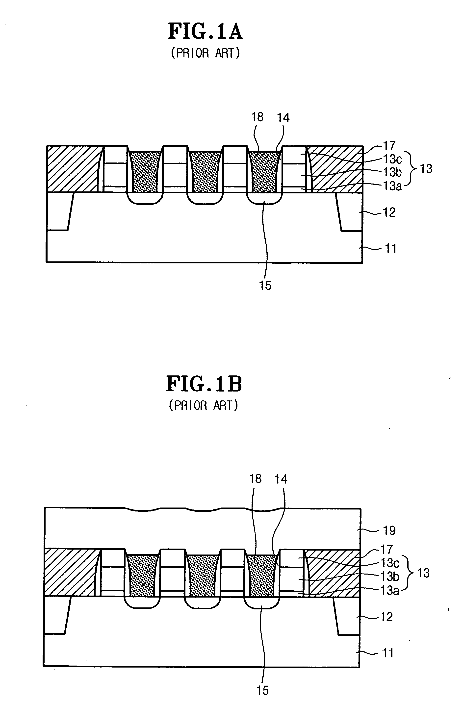
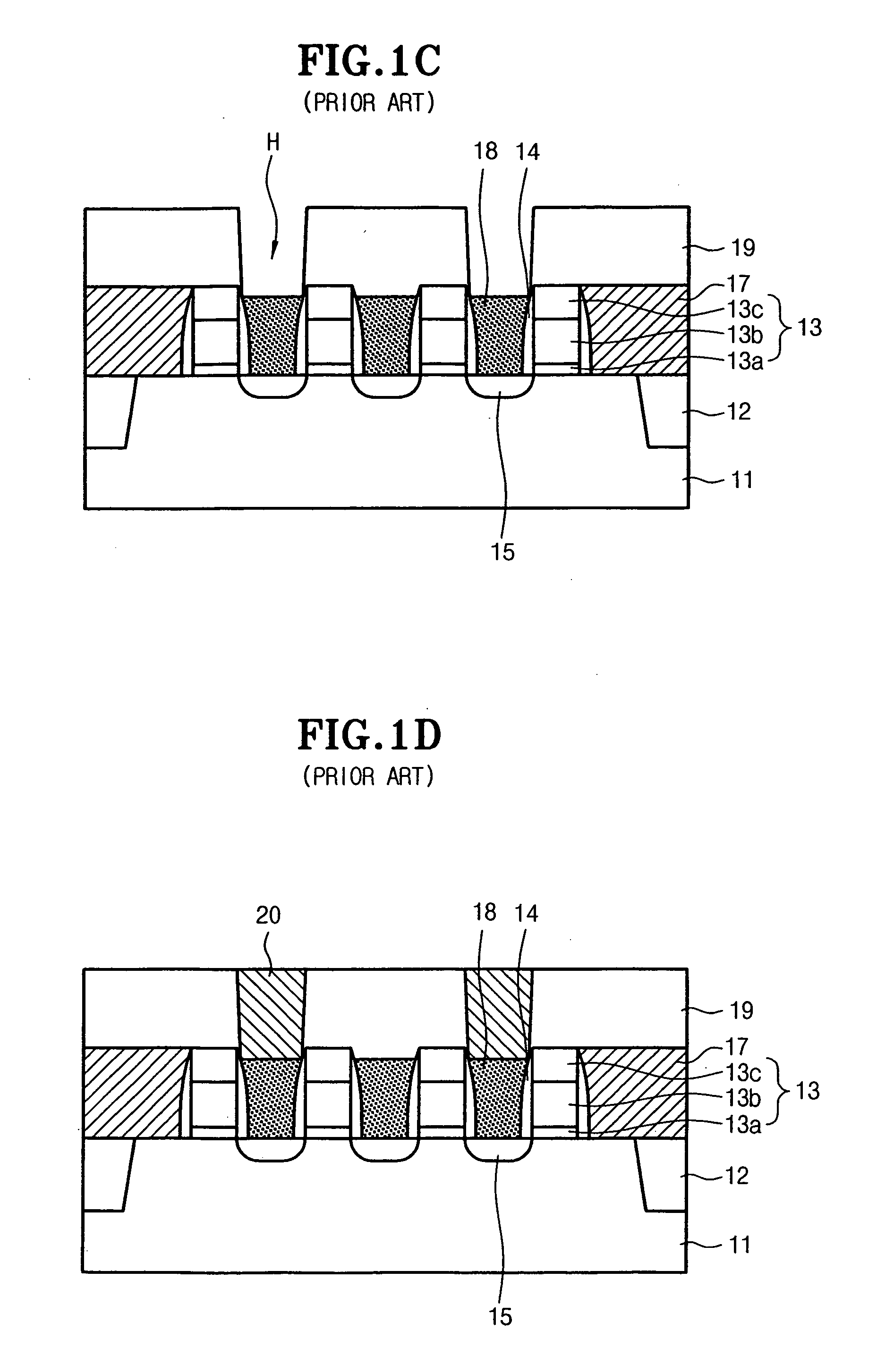
[0020] Hereinafter, a preferred embodiment of the present invention will be described with reference to the accompanying drawings. In the following description and drawings, the same reference numerals are used to designate the same or similar components, and so repetition of the description on the same or similar components will be omitted.

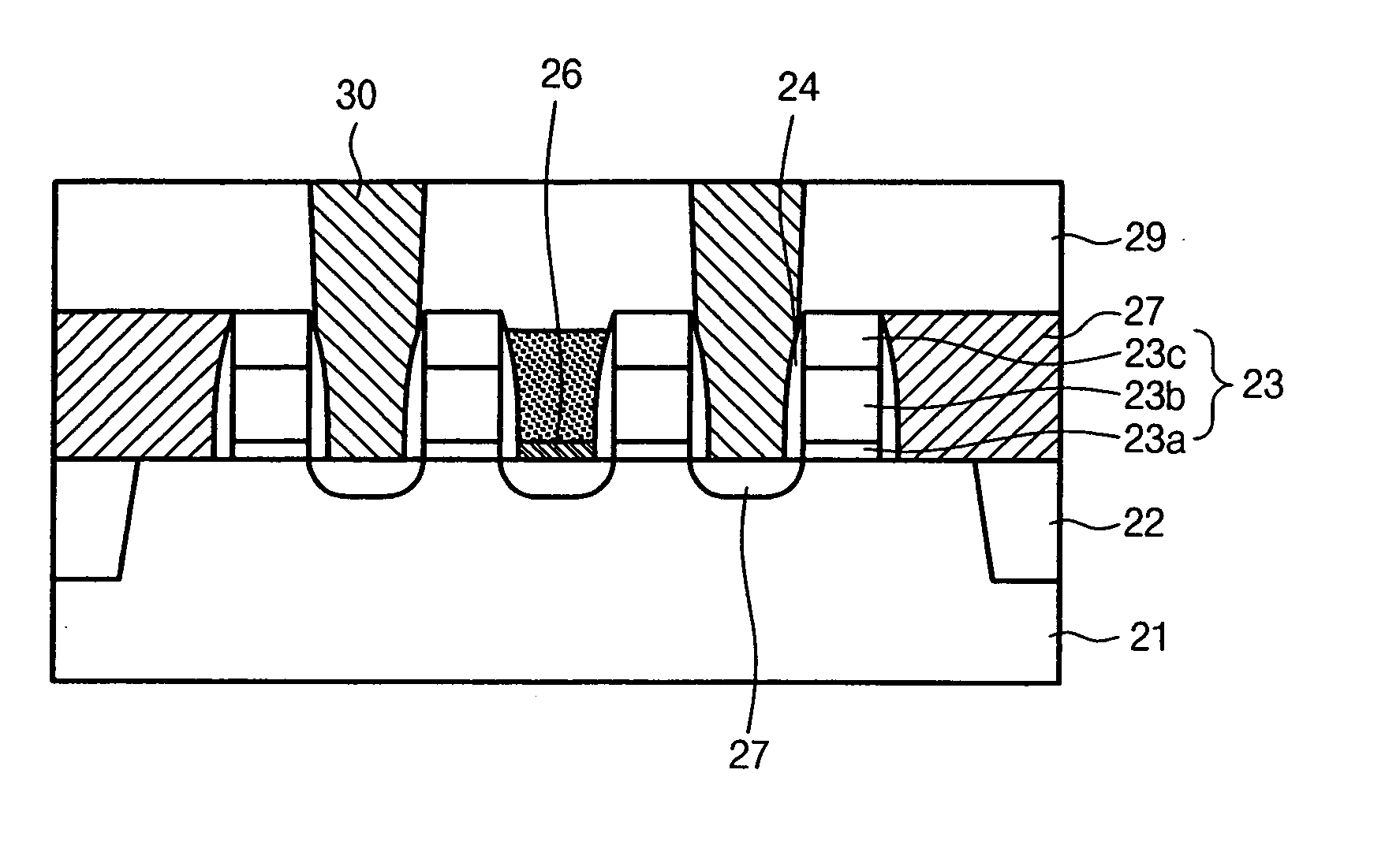
[0021]FIGS. 2A to 2E illustrate process-by-process sectional view for explaining a method for forming a storage node contact of a semiconductor device in accordance with a preferred embodiment of the present invention.

[0022] Referring to FIG. 2A, a gate insulating film 23a, a gate conductive film 23b and a nitride film 23c as a hard mask are successively formed on a semiconductor substrate 21 on which a device separating film 22 has been formed, and then are patterned to form gates 23. Thereafter, an insulating film is deposited and blanket-etched to form spacers 24 on both sidewalls of the respective gates 23 and then impurities are ion-implan...


PUM


Abstract

Disclosed is a method for forming a storage node contact of a semiconductor device. In such a method, there is provided a substrate formed with gates and source/drain regions. A landing plug poly is formed between the gates, and an insulating interlayer is formed over the entire surface of the substrate including the landing plug poly and the gates. The insulating interlayer is then etched to form a storage node contact hole exposing the landing plug poly. Thereafter, the landing plug poly exposed through the storage node contact hole is removed. Finally, a polysilicon film is filled up within a vacant portion from which the landing plug poly is removed and the storage node contact hole above the vacant portion.

Description

BACKGROUND OF THE INVENTION [0001] 1. Field of the Invention [0002] The present invention relates generally to a method for manufacturing a semiconductor device, and more particularly to a method for forming a storage node contact of a semiconductor device, which can improve contact resistance while preventing misalignment between a landing plug poly and the storage node contact. [0003] 2. Description of the Prior Art [0004] As an area available for forming a pattern decreases and a level difference increases due to high integration of semiconductor devices, it has become difficult to form a contact between a storage node and a substrate. Thus, in order to solve process difficulties caused by a high level difference, that is, in order to ensure a contact margin between a storage contact and a substrate, there has been universalized a technology in which a storage node contact is formed prior to the formation of the storage node. [0005] Hereinafter, a conventional method for forming ...

Claims


Application Information

Patent Timeline
IPC IPC(8): H01L21/4763H01L21/44
CPCH01L21/76895H01L21/76877H01L21/28
Inventor AHN, HYUNLEE, JU HEE
Owner SK HYNIX INC
Why Eureka
Try Eureka