
Group iii nitride semiconductor device

Inactive Publication Date: 2011-07-21
SUMITOMO ELECTRIC IND LTD
View PDF11 Cites 4 Cited by
  • Summary
  • Abstract
  • Description
  • Claims
  • Application Information

AI Technical Summary

Benefits of technology

[0047]The below will describe the advantageous effects achieved by the Group III nitride semiconductor device and its fabrication method of the present embodiment described above.
[0048]The inventors attempted to form an electrode on a nonpolar or semipolar plane of GaN, using the conventional technology (Patent Literatures 1 and 2) for forming the ohmic electrode on the c-plane of GaN crystal. However, for example, when Ni / Au metal film was formed on a nonpolar or semipolar plane of GaN, e.g., a (11-22) plane and the metal film was alloyed in an oxygen atmosphere, the contact resistance of the ohmic electrode was not reduced. When a Pt electrode was made on a nonpolar or semipolar plane at high temperature as in the other conventional technology (Patent Literatures 3 and 4), no ohmic contact was achieved. Namely, it became clear that these conventional technologies allowed a good ohmic electrode to be formed on the c-plane of GaN crystal, but hardly allowed a good ohmic electrode to be formed on a nonpolar plane or a semipolar plane.
[0049]Then, the inventors produced a Pd electrode on a nonpolar plane and a semipolar plane of GaN crystal at low temperature. As a result, a goad ohmic contact was achieved. For finding the reason for it, a surface analysis was conducted with an X-ray photoelectron spectrometer (XPS). It was confirmed by this analysis that the Pd electrode formed at low temperature on the nonpolar or semipolar plane of GaN crystal provided a sub-peak which was not observed with the other electrodes. It is considered that a transition layer resulting from interdiffusion of Pd and GaN was newly made between the nonpolar or semipolar plane of GaN crystal and the Pd electrode and it improved the contact resistance between the GaN crystal and the Pd electrode. A bonding state of a crystal surface on the nonpolar or semipolar plane is different from that on the c-plane. GaN and Pd are likely to bind to each other on the nonpolar or semipolar plane. It is thus presumed that the transition layer as described above spread at the interface between the GaN crystal and the Pd electrode. This phenomenon is considered to occur in the same manner in the Group III nitride semiconductors other than GaN.
[0050]In this embodiment, as described above, the semiconductor region 13 has the surface 13a, which is nonpolar or semipolar. As the metal electrode 17 containing Pd is formed on the surface 13a, the transition layer 19 is made. The transition layer 19 improves adhesion between the semiconductor region 13 and the metal electrode 17, so as to decrease the contact resistance between them.
[0051]The thickness of the transition layer 19 is preferably more than or equal to 0.5 nm and less than or equal to 3 nm. The inventors investigated a relation between the thickness of the transition layer 19 and electrical characteristics. As a result, good electrical characteristics were obtained in the thickness range of more than or equal to 0.5 nm and less than or equal to 3 nm. Namely, the contact resistance can be more effectively reduced by the transition layer 19 in such thickness.
[0052]The metal electrode 17 preferably contains Pd. The reason for it is that the transition layer 19 is suitably made between the metal electrode 17 and the semiconductor region 13 when the metal electrode 17 contains Pd. It is, however, noted that the metal to form the transition layer 19 is not limited only to Pd. For example, the transition layer can be made by the metal electrode containing Pt.

Problems solved by technology

Since the diameter of indium atom is larger than the diameter of gallium atom, increase in the indium composition leads to increase in internal strain in the indium-containing layer because of lattice mismatch.
As a result, a large piezoelectric field is induced in the layer, so as to decrease the recombination probability and thus reduce the luminous efficiency.

Method used


Image

  • Group iii nitride semiconductor device
  • Group iii nitride semiconductor device
  • Group iii nitride semiconductor device

Examples


example 1

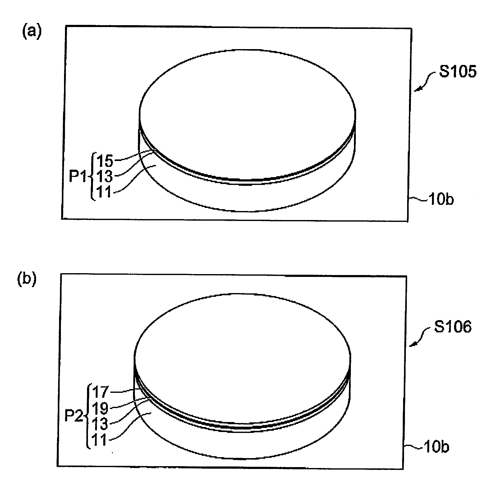
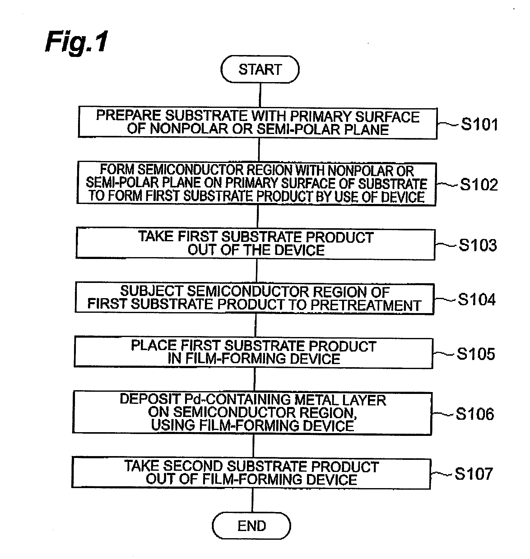
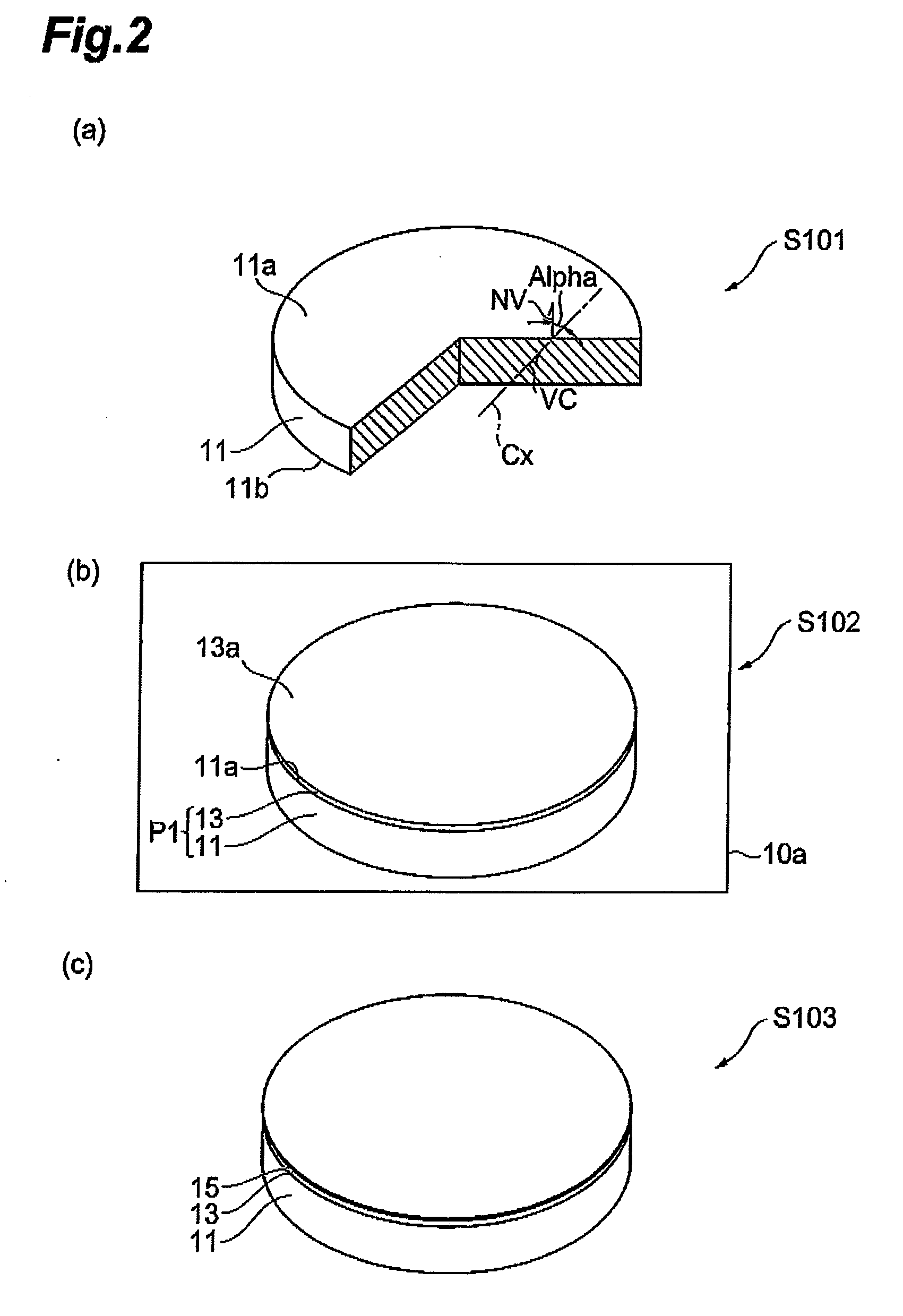
[0054]An epitaxial substrate shown in FIG. 4A was produced by organometallic vapor phase epitaxy using an n-type semipolar GaN substrate 31. The primary surface of the GaN substrate 31 included an m-plane. An n-type GaN buffer layer 32 was formed on this primary surface. The epitaxial substrate Epi1 included a Si-doped n-type GaN layer 33, a Mg-doped GaN layer 34, and a high-concentration Mg-doped p-type GaN layer 35. The thickness of the Si-doped n-type GaN layer 33 was 1 μm. The thickness of the Mg-doped GaN layer 34 was 0.4 μm. The thickness of the high-concentration Mg-doped p-type GaN layer 35 was 50 nm. These GaN-based semiconductor layers were grown in order on the substrate 31.

[0055]A resist was then formed by photolithography, prior to deposition of a metal film for a p-type electrode. This resist had an annular aperture. Thereafter, a Pd electrode was evaporated onto the epitaxial substrate by the electron beam method, in an evaporation system in vacuum of about 1×10⁻⁶ Tor...

example 2

[0057]An epitaxial substrate was produced according to the same procedure as in Example 1. This epitaxial substrate was subjected to ultrasonic organic cleaning using acetone and 2-propanol. Thereafter, it was cleaned with hydrochloric acid, aqua regia, and hydrofluoric acid, for five minutes each. A Pd electrode was evaporated onto this epitaxial substrate by the electron beam method. The thickness of the Pd electrode was 100 Å. The temperature during the evaporation was room temperature. On the other hand, another epitaxial substrate was prepared by the production and cleaning methods of the same steps as the above epitaxial substrate. An Ni / Au electrode was evaporated onto this epitaxial substrate. Then this Ni / Au electrode was subjected to a thermal treatment. Ni was evaporated by the electron beam method. Au was evaporated by resistive heating. The thickness of each of Ni and Au layers was 50 Å. In this manner, the different types of p-type electrodes were made on the two respe...


PUM


Abstract

A Group III nitride semiconductor device has a semiconductor region, a metal electrode, and a transition layer. The semiconductor region has a surface comprised of a Group III nitride crystal. The semiconductor region is doped with a p-type dopant. The surface is one of a semipolar surface and a nonpolar surface. The metal electrode is provided on the surface. The transition layer is formed between the Group III nitride crystal of the semiconductor region and the metal electrode. The transition layer is made by interdiffusion of a metal of the metal electrode and a Group III nitride of the semiconductor region.

Description

BACKGROUND OF THE INVENTION[0001]1. Field of the Invention[0002]The present invention relates to a Group III nitride semiconductor device.[0003]2. Related Background Art[0004]Patent Literatures 1 and 2 describe a method for forming an ohmic electrode on a p-type gallium nitride (GaN) layer grown on a (0001) plane or c-plane. In this method, Ni / Au film is evaporated onto the p-type GaN layer and thereafter a thermal treatment is carried out in an oxygen atmosphere. An oxide film exists on the surface of the p-type GaN layer, but nickel absorbs the oxide film by this method. Then nickel binds to oxygen atoms of the oxide film, thereby removing the oxide film. This allows gold to come into contact with the p-type GaN crystal, thereby forming an ohmic contact.[0005]Patent Literature 3 describes the result of an experiment. In this experiment, a p-type Group III nitride semiconductor layer is grown on a sapphire substrate. Then the substrate is heated to 300° C. and thereafter platinum o...

Claims


Application Information

Patent Timeline
IPC IPC(8): H01L29/20
CPCH01L21/28575H01L29/2003H01L29/045H01L33/32H01L33/40H01L29/452H01L33/16H01L33/36
Inventor TOKUYAMA, SHINJIUENO, MASAKIADACHI, MASAHIROKYONO, TAKASHISUMITOMO, TAKAMICHIKATAYAMA, KOJISAITO, YOSHIHIRO
Owner SUMITOMO ELECTRIC IND LTD
Features
  • Generate Ideas
  • Intellectual Property
  • Life Sciences
  • Materials
  • Tech Scout
  • Unparalleled Data Quality
  • Higher Quality Content
  • 60% Fewer Hallucinations
Learn More