

Method for fabricating capacitor in semiconductor device
- Summary
- Abstract
- Description
- Claims
- Application Information
AI Technical Summary
Benefits of technology
Problems solved by technology
Method used
Image

Examples
Embodiment Construction
[0011]Other objects and advantages of the present invention can be understood by the following description, and become apparent with reference to the embodiments of the present invention.
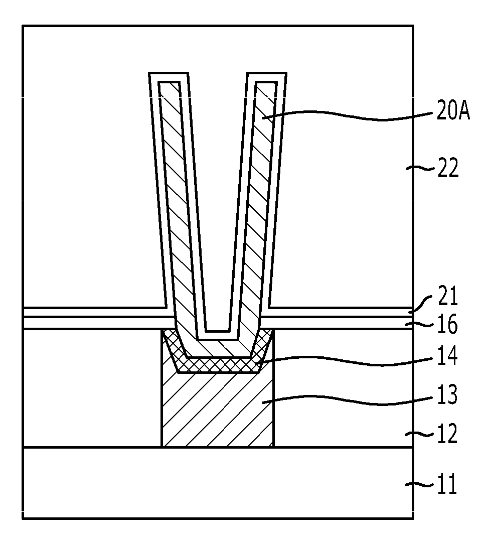
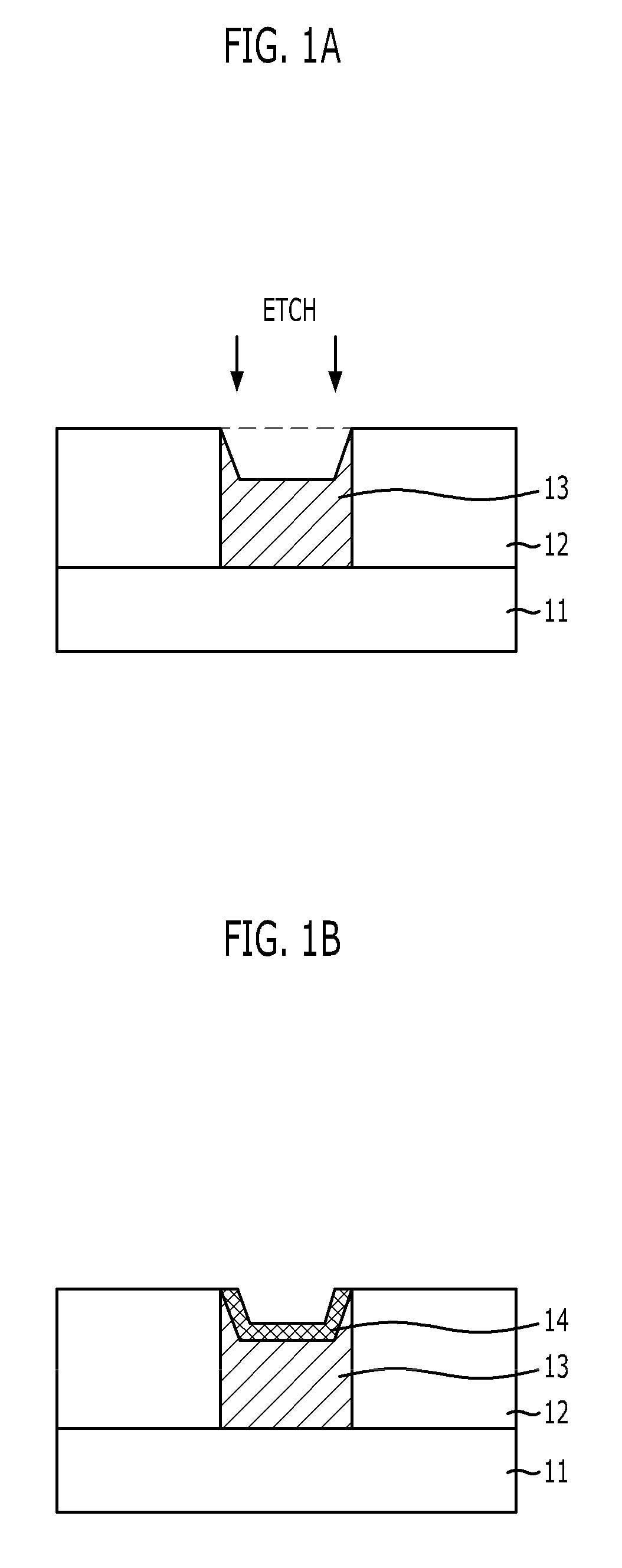
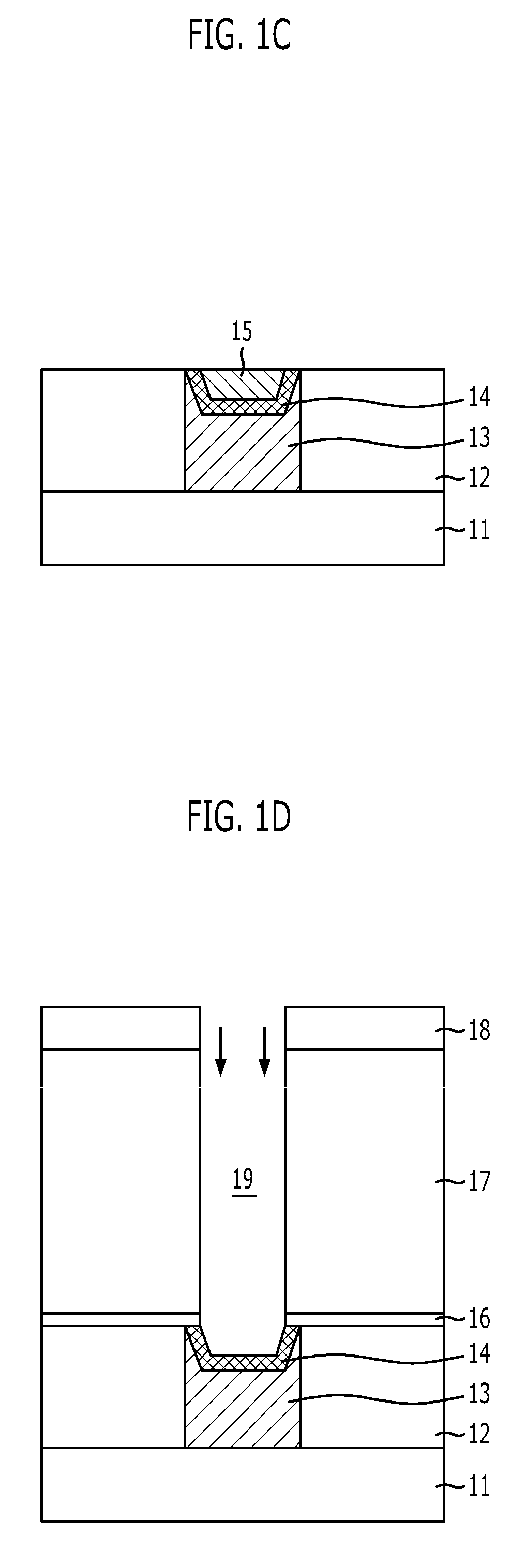
[0012]Embodiments of the present invention relate to a method for fabricating a capacitor in a semiconductor device. According to the embodiments, a storage node contact plug is recessed to a certain depth to have a sloped profile and a barrier metal is formed over the recessed storage node contact plug so that a contact area increases by as much as the sloped profile, thereby reducing a contact resistance.
[0013]Furthermore, a bottom electrode is formed after forming a barrier metal over a recessed storage node contact plug so that a storage capacity (Cs) is secured by as much as the recessed portion of the storage node contact plug without increasing the height of a capacitor. Also, recessing the storage node contact plug provides a greater supporting strength at the bottom than when forming a bott...
PUM
 Abstract
Description
Claims
Application Information