Method for Stacking Semiconductor Chips

a technology of semiconductor chips and stacking methods, which is applied in the direction of semiconductor devices, semiconductor/solid-state device details, electrical equipment, etc., can solve the problems of increasing the complexity of the product, the cost per functional unit should drop, and the increase of the functional complexity paralleled by the equivalent increase in the reliability of the produ

Active Publication Date: 2009-03-26
TEXAS INSTR INC
View PDF4 Cites 41 Cited by
  • Summary
  • Abstract
  • Description
  • Claims
  • Application Information

AI Technical Summary

Benefits of technology

[0009]This invention solves the problem by using “low impact” regions around the periphery of the chip to position metal-filled vias, preferably in linear or staggered arrays. These regions also contain the chip bond pads so that the vias can be elect

Problems solved by technology

First, the higher product complexity should largely be achieved by shrinking the feature sizes of the chip components while holding the package dimensions constant; preferably, even the packages should shrink.
Second, the increased functional complexity should be paralleled by an equivalent increase in reliability of the product.
Third, the cost per functional unit should drop with each generation of complexity so that the cost of the product with its doubled functionality would increase only slightly.
The achievable bump pitch, how

Method used


Image

  • Method for Stacking Semiconductor Chips
  • Method for Stacking Semiconductor Chips
  • Method for Stacking Semiconductor Chips

Examples


Embodiment Construction

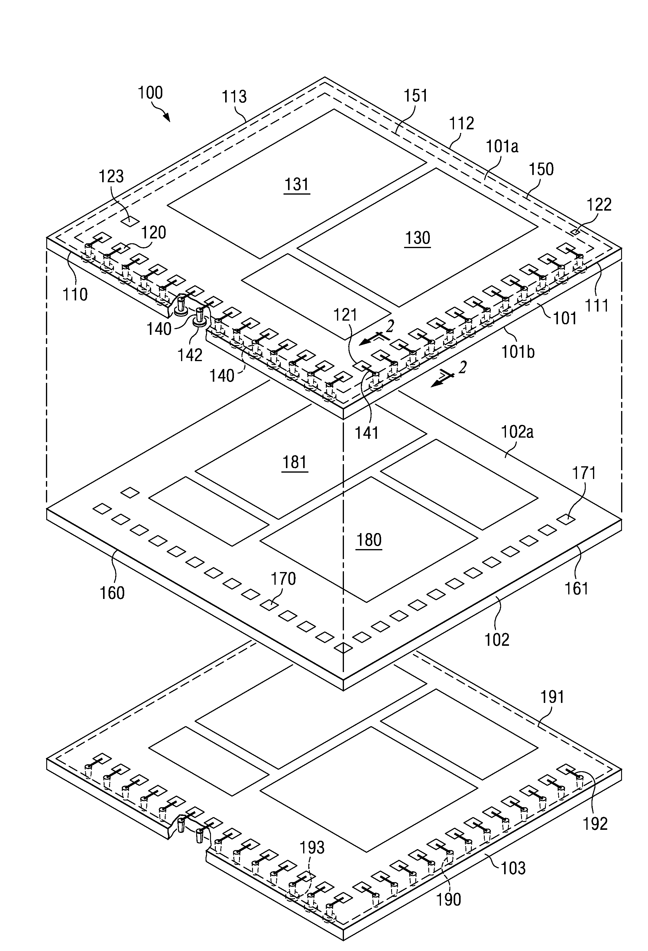
[0031]FIG. 1 depicts an embodiment of the invention; the schematic perspective view shows two semiconductor chips 101 and 102 to be assembled into a chip stack generally designated 100. The top chip 101 and the bottom chip 102 exhibit features according to the invention, which facilitate the stack assembly without the need for redesigning the circuitry of either chip. As a consequence, the assembly of the chip-stack product 100 creates a device, which combines the characteristics of existing chip 101 as well as existing chip 102 without spending the effort, time and cost to design the new device or to modify the circuitry of either chip.

[0032]Semiconductor chip 101 has edges 110, 111, 112, and 113; it further has first surface 101a and second surface 101b. First surface 101a includes first contact pads 120 near edge 110, contact pads 121 near edge 111, contact pads 122 near edge 112, and contact pads 123 near edge 113. Chip 101 has active components, such as integrated circuits 130 ...


PUM


Abstract

In a semiconductor system (100) including a chip (101) and a workpiece (102), the chip has metal-filled vias (140) positioned between contact pads (120) and the respective edges (110). In addition, seals against microcracks (150) and thermo-mechanical stress (151) are located between the vias and the active components, and sometimes also between the vias and the respective nearest edge. Workpiece (102) may be another semiconductor chip or a substrate; it has contact pads (170) matching the locations of the vias (140). The chip is vertically stacked on the workpiece so that each contact pad (170) is aligned and in electrical contact with the corresponding via (140).

Description

FIELD OF THE INVENTION[0001]The present invention is related in general to the field of semiconductor devices and processes and more specifically to the structure and fabrication method of vertically stacked and horizontally joined semiconductor chips.DESCRIPTION OF THE RELATED ART[0002]The long-term trend in semiconductor technology to double the functional complexity of its products every 18 months (Moore's “law”) has several implicit consequences. First, the higher product complexity should largely be achieved by shrinking the feature sizes of the chip components while holding the package dimensions constant; preferably, even the packages should shrink. Second, the increased functional complexity should be paralleled by an equivalent increase in reliability of the product. Third, the cost per functional unit should drop with each generation of complexity so that the cost of the product with its doubled functionality would increase only slightly.[0003]As for the challenges in semi...

Claims


Application Information

Patent Timeline
IPC IPC(8): H01L23/48H01L21/58
CPCH01L21/563H01L23/481H01L2924/0002H01L2924/10253H01L2225/1058H01L23/49816H01L23/585H01L24/05H01L24/13H01L24/16H01L24/17H01L25/0655H01L25/0657H01L25/105H01L25/50H01L2224/0557H01L2225/06513H01L2225/06541H01L2225/06551H01L2924/01079H01L2924/14H01L2924/15311H01L2924/15331H01L2924/30107H01L2924/3025H01L25/03H01L2225/1023H01L2924/00H01L2224/05552H01L2224/0401
Inventor GERBER, MARK A.
Owner TEXAS INSTR INC
Why Eureka
Try Eureka