Unlock instant, AI-driven research and patent intelligence for your innovation.

Erase method in thin film nonvolatile memory

a non-volatile memory, erase method technology, applied in static storage, digital storage, instruments, etc., can solve the problems of reducing the efficiency of boosting, memory cell by memory cell erase operation is very slow for practical use, and the non-volatile memory cell erase operation has arisen. , to achieve the effect of optimizing scalability and fast eras

Inactive Publication Date: 2009-03-26
SCHILTRON
View PDF14 Cites 6 Cited by
  • Summary
  • Abstract
  • Description
  • Claims
  • Application Information

AI Technical Summary

Benefits of technology

[0018]An erase method of the present invention is applicable to dual-gate memory strings. Such a method has key advantages over erase methods for other thin-film non-volatile memory strings. The advantages include (a) fast erase without any source-to-body short; (b) flexible erase which erases any number of memory cells in a block (i.e., from none to all memory cells in the block); (c) source voltage may be set to optimize non-selected string channel boosting; and (d) the thickness of the thin-film device's body can be optimized for scalability. The method uses the access devices of the dual-gate memory cells in a memory string to form inversion channels, so as to provide conductive paths for the memory cells to be erased to a node at a more positive voltage than the erase voltage applied to the gate electrodes of the memory devices to be erased.

Problems solved by technology

Erasing non-volatile memory cells has arisen as a problem in series-connected thin-film transistors that act as non-volatile memory devices (e.g., the NAND memory string configuration shown in the Jung Article).
Such a memory cell by memory cell erase operation is very slow for practical use.
The leakage current reduces the efficiency of the boosting.
Capacitive boosting, however, is not possible in the memory strings of the Jung Article, as illustrated in FIGS. 5 and 6.
Because the method requires other memory devices to provide the inversion channels, simultaneously erasing of multiple memory cells is practically impossible (or at least requiring a prohibitively long time).
There are several disadvantages associated with the erase operation of FIG. 6:(1) The CSL contact must remain close to the ground reference during a programming operation and cannot be taken to a positive voltage (e.g., 3V or above) because a positive source line voltage would require the same voltage be placed on the bit line contact in the selected memory string.
Generating such a high voltage in the memory string is undesirable.(2) Maintaining the CSL at close to ground potential during programming results in a large voltage drop in the non-selected NAND string between the capacitively boosted channel and the grounded CSL across the length of the source line select device.
A leakage current may develop to cause a droop in the boosted voltage in a non-selected string.
The droop in voltage can result in program disturb.
However, this approach may lead to other leakage effects (e.g., gate-induced drain leakage (GIDL)).(3) Shorting the source N+ region to the active p-type semiconductor region is accomplished by providing the CSL contact that penetrates through to the active p− region.
Consequently, the thicknesses of the active silicon regions of thin film devices—an important parameter for good scalability—cannot be freely adjusted.

Method used


Image

  • Erase method in thin film nonvolatile memory
  • Erase method in thin film nonvolatile memory
  • Erase method in thin film nonvolatile memory

Examples


Embodiment Construction

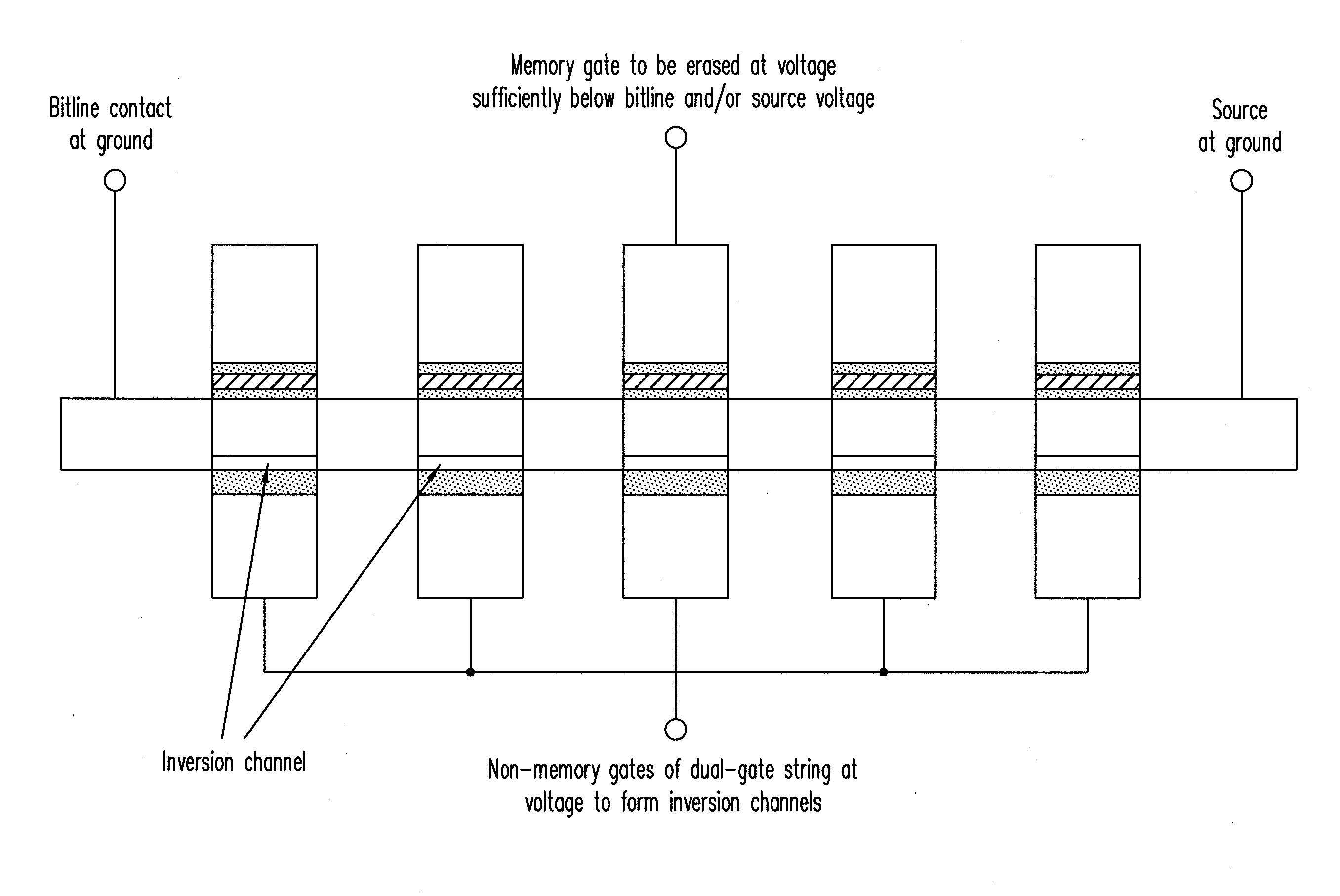
[0027]FIG. 1 is a cross-section of dual-gate memory cell 100 formed by a memory device and a non-memory device (also, referred to as an “access device”). As shown in FIG. 1, the access device includes gate dielectric 106 and gate electrode 102 and the memory device includes gate dielectric stack 108 and gate electrode 109. The memory and access devices share source and drain regions 110 and active region 107. Although shown having the memory device formed above the access device, these device may be formed in the reverse order—i.e., with the memory device formed underneath the access device. FIG. 2 is a graphical representation 200 of a dual-gate device, indicating gate electrode 201 of the memory device, and gate electrode 202 of the access device, with source and drain connections 203 and 204.

[0028]FIG. 3 shows memory strings 501 and 502 each formed out of serially connected dual-gate memory cells provided between dual-gate select devices provided at the ends of the memory string....


PUM


Abstract

An erase method applicable to dual-gate memory strings has key advantages over erase methods for other thin-film non-volatile memory strings. The advantages include (a) fast erase without any source-to-body short; (b) flexible erase which erases any number of memory cells in a block (i.e., from none to all cells); (c) source voltage may be set to optimize non-selected string channel boosting; and (d) the thickness of the thin-film device's body can be optimized for scalability. The method uses the access devices of the dual-gate memory cells in a memory string to form inversion channels, so as to provide conductive paths between the memory cells to be erased and a node at a more positive voltage than the erase voltage applied to the gate electrodes of the memory devices to be erased.

Description

CROSS-REFERENCE TO RELATED APPLICATIONS[0001]The present patent application is related to and claims priority of U.S. provisional patent application (“Provisional Application”), entitled “Erase Method in Thin Film Nonvolatile Memory,” Ser. No. 60 / 974,429, which was filed on Sep. 21, 2007. The present invention is also related to U.S. patent applications (“Copending Applications”), both entitled “Dual Gate Device and Method,” Ser. Nos. 11 / 197,462 and 11 / 548,231, filed on Aug. 3, 2005 and Oct. 10, 2006, respectively.[0002]The Provisional Application and the Copending Applications are hereby incorporated herein by reference in their entireties.BACKGROUND OF THE INVENTION[0003]1. Field of the Invention[0004]The present invention relates to erase methods in non-volatile memories. In particular, the present invention relates to erase methods in dual-gate memory cells organized into memory strings.[0005]2. Discussion of the Related Art[0006]Thin-film transistors have been proposed as build...

Claims


Application Information

Patent Timeline
IPC IPC(8): G11C16/14G11C16/04
CPCG11C16/16G11C16/0483
Inventor WALKER, ANDREW J.
Owner SCHILTRON