Memory device based on phase change quantum dots and manufacturing method thereof

A storage device and quantum dot technology, which is applied in the field of storage devices based on phase-variable quantum dots and their preparation, can solve problems such as single storage state, and achieve the effects of increasing the amount of charge storage and improving the accuracy of information storage.

Inactive Publication Date: 2014-07-09
SHAOXING UNIVERSITY
View PDF3 Cites 3 Cited by
  • Summary
  • Abstract
  • Description
  • Claims
  • Application Information

AI Technical Summary

Problems solved by technology

[0003] In order to overcome the problem of single storage state in the prior art, the presen...

Method used


Image

  • Memory device based on phase change quantum dots and manufacturing method thereof
  • Memory device based on phase change quantum dots and manufacturing method thereof
  • Memory device based on phase change quantum dots and manufacturing method thereof

Examples


Embodiment Construction

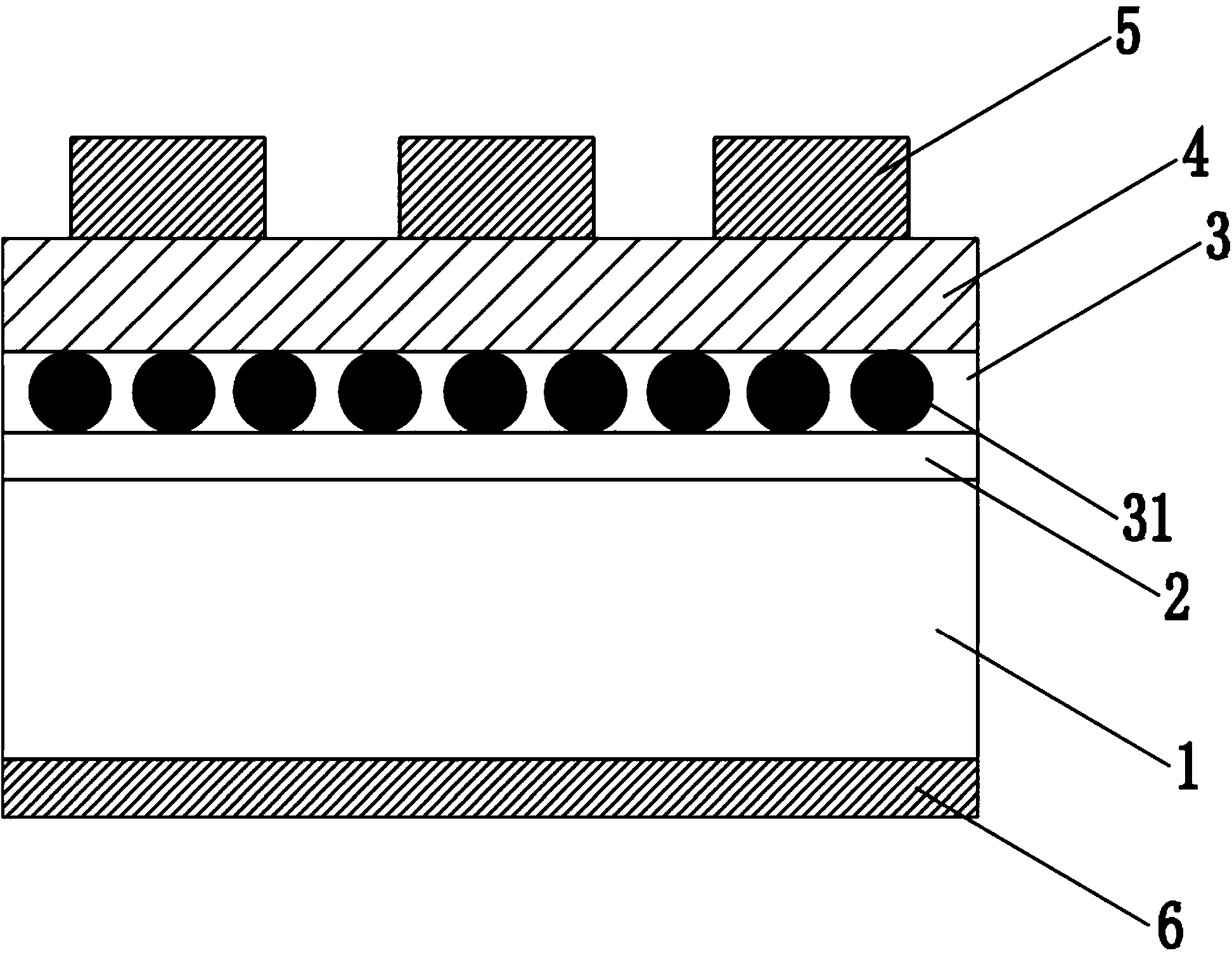
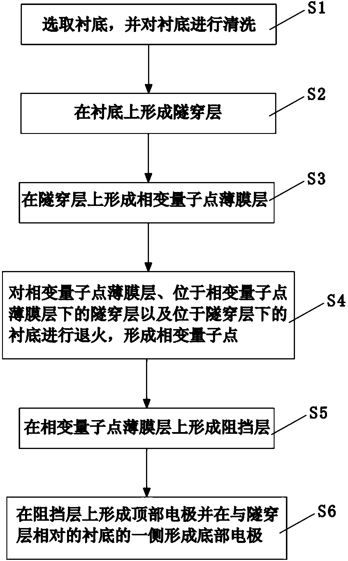
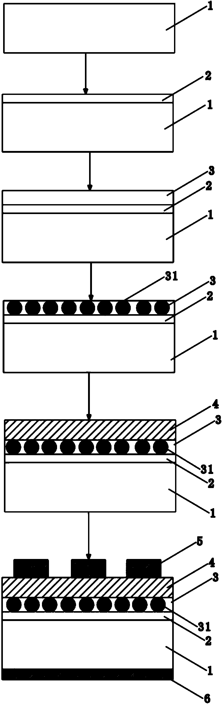
[0020] figure 1 Shown is a cross-sectional structure diagram of a storage device based on phase variable quantum dots provided by an embodiment of the present invention. figure 2 Shown is a flowchart of a method for fabricating a storage device based on phase variable quantum dots provided by an embodiment of the present invention. image 3 Shown is a process schematic diagram of a storage device manufacturing method based on phase change quantum dots provided by an embodiment of the present invention. Please also refer to Figure 1 to Figure 3 .

[0021] The storage device based on phase transition quantum dots provided by the present invention includes a semiconductor substrate 1 , a tunneling layer 2 , a phase transition quantum dot film layer 3 , a barrier layer 4 , a first electrode 5 and a second electrode 6 . The tunneling layer 2 is disposed on the semiconductor substrate 1 . The phase transition quantum dot thin film layer 3 is arranged on the tunneling layer 2, ...


PUM

PropertyMeasurementUnit
Thicknessaaaaaaaaaa
Thicknessaaaaaaaaaa
Thicknessaaaaaaaaaa

Abstract

The invention discloses a memory device based on phase change quantum dots and a manufacturing method of the memory device. The memory device based on the phase change quantum dots comprises a semiconductor substrate, a tunneling layer, a phase change quantum dot film layer, a barrier layer, a first electrode and a second electrode. The tunneling layer is arranged on the semiconductor substrate; the phase change quantum dot film layer is arranged on the tunneling layer and comprises the phase change quantum dots, and the phase change quantum dots can achieve information storage through trapping tunneling charges and reversible transformation between a crystalline state and an amorphous state; the barrier layer is arranged on the phase change quantum dot film layer and can stop charges trapped by the phase change quantum dots from entering the first electrode; the first electrode supplies electricity to the barrier layer; the second electrode supplies electricity to the semiconductor substrate.

Description

Background technique [0001] With the rapid development of the consumer electronics market in recent years, the memory market, which is an important part of the semiconductor and information industries, is getting bigger and bigger. At present, the mainstream memory in the market is DRAM and flash memory. Although the DRAM has the advantages of high capacity and low cost, the data of the DRAM cannot be saved after the power supply is turned off, which limits the application range of the DRAM. In addition, after the feature size of DRAM is reduced to close to 45 nanometers, the requirements for materials are very high. It is necessary to use ultra-high dielectric constant materials with a dielectric constant greater than 700 to maintain a sufficiently high capacitance. Although flash memory is a non-volatile storage technology, flash memory also has disadvantages such as high power consumption, poor radiation resistance, short cycle life, and limitations in size reduction. [...

Claims


Application Information

Patent Timeline
IPC IPC(8): H01L45/00H01L27/04
Inventor 倪鹤南吴良才李志彬王艳智龚路鸣
Owner SHAOXING UNIVERSITY
Why Eureka
Try Eureka