

Two-bit flash memory
a two-bit flash memory and memory cell technology, applied in the direction of semiconductor devices, electrical apparatus, transistors, etc., can solve the problems of insufficient memory cell windows and greatly reduced and achieve the effect of increasing the controllability of the control ga
- Summary
- Abstract
- Description
- Claims
- Application Information
AI Technical Summary
Benefits of technology
Problems solved by technology
Method used
Image

Examples
first embodiment
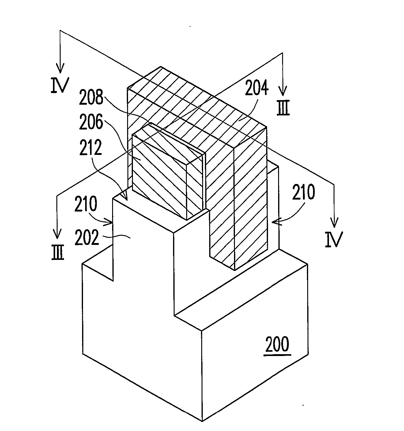
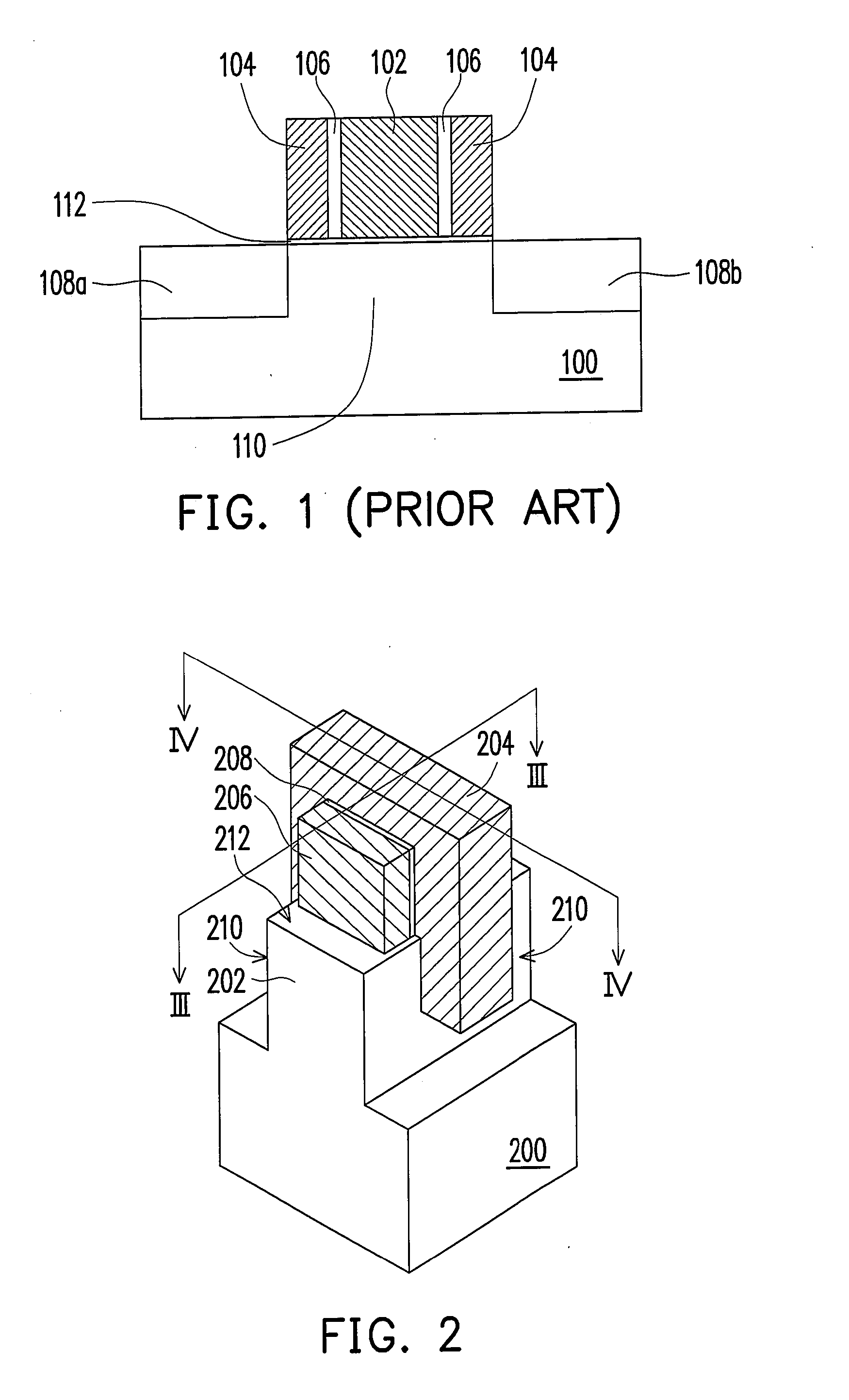
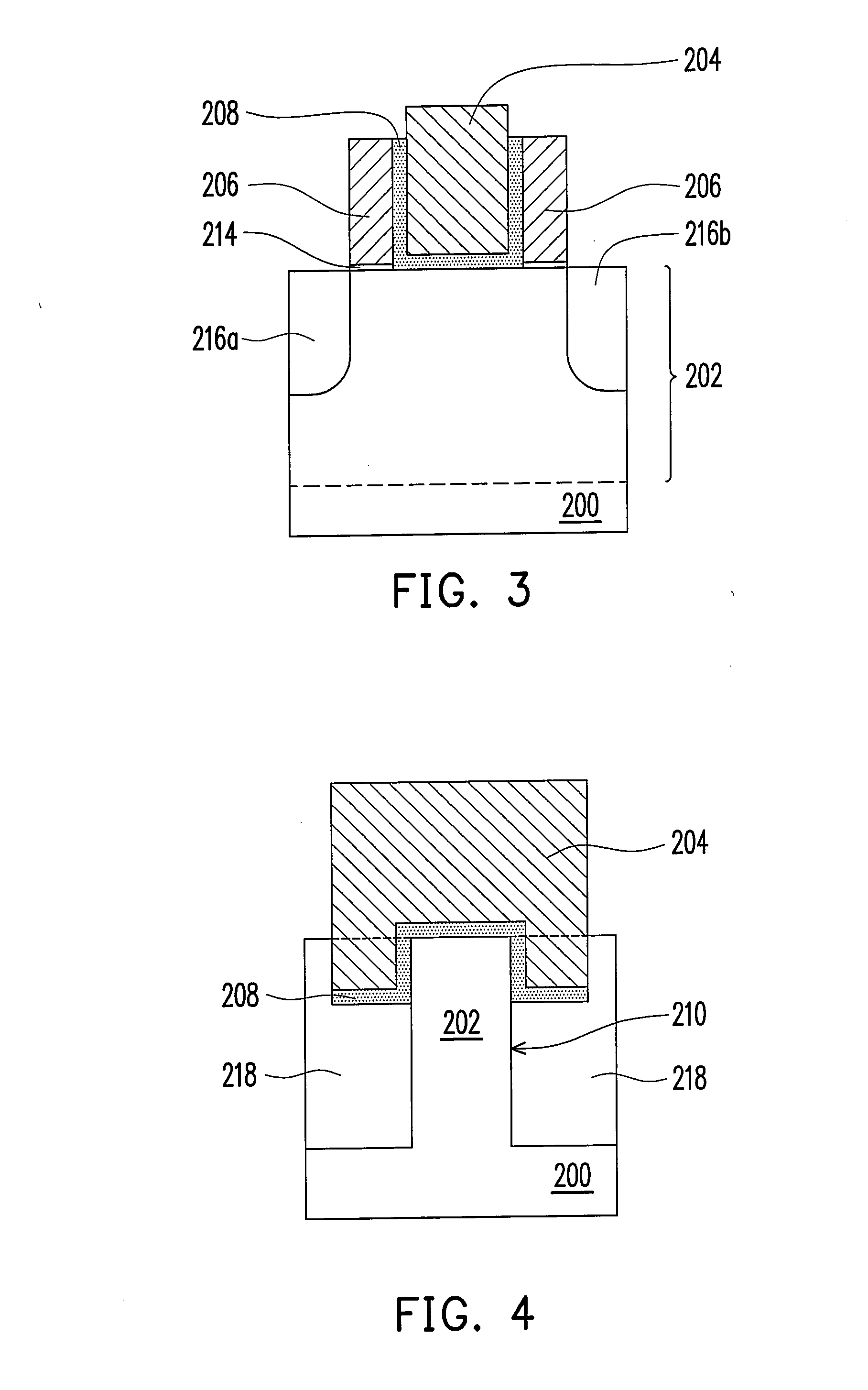
[0033]FIG. 2 is a perspective structural view of a flash memory according to the present invention, in which a part of the components are omitted to make the drawing clearer. FIG. 3 is a cross-sectional view taken along a line segment III-III in FIG. 2, and FIG. 4 is a cross-sectional view taken along a line segment IV-IV in FIG. 2.
[0034]Firstly, referring to FIG. 2, the flash memory of the first embodiment includes a substrate 200 having a protrusion 202 extending from a top face of the substrate 200, an control gate 204, two floating gates 206, and a dielectric layer 208. The control gate 204 in the drawing is formed on the protrusion 202 of the substrate 200 and extendedly covers two opposite sidewalls 210 of the protrusion 202. The floating gates 206 are respectively formed on top of the protrusion 202 of the substrate 200 and being on two opposite sides of the control gate 204. The dielectric layer 208 is sandwiched by the control gate 204 and the floating gates 206. The floati...
second embodiment
[0040]FIGS. 6A to 6H are perspective views of a flow for manufacturing a flash memory according to the present invention.
[0041]Referring to FIG. 6A, a substrate 600 is provided, which has a plurality of isolation structures 602, for example, STI structures. A protrusion 604 of the substrate 600 is sandwiched by the isolation structures 602.
[0042]Next, referring to FIG. 6B, a thin insulating layer 606 is formed on the surface of the protrusion 604, and then a first conductor layer 608 extending towards a first direction is further formed on the insulating layer 606.
[0043]Then, referring to FIG. 6C, a dielectric layer 610 is formed on the isolation structures 602, and the dielectric layer 610 is approximately at a same level with the top surface of the first conductor layer 608. Then, a first mask layer 612 is formed on the substrate 600, for covering the dielectric layer 610 and the first conductor layer 608, in which the first mask layer 612 may be made of photoresist, silicon nitri...
third embodiment
[0049]FIG. 7 is a perspective structural view of a flash memory according to the present invention.
[0050]Referring to FIG. 7, the flash memory of the third embodiment includes a substrate 700 having a channel region 702, a source 704a and a drain 704b, two floating gates 706, a control gate 708, an insulating layer 718 and a dielectric layer 710. In the third embodiment, the channel region 702 includes a first set of two opposite sides 712 and a second set of two opposite sides 714 in the substrate 700, wherein the first set of two opposite sides 712 are orthogonal to the second set of two opposite sides 714, for example. The source 704a and the drain 704b are respectively formed on the first set of two opposite sides 712 of the channel region 702. The two floating gates 706 are respectively formed on two opposite sidewalls of the control gate 708 and on top of the channel region 702, which may be disposed on the substrate 700 as shown in the drawing, or may be disposed in the subst...
PUM
 Abstract
Description
Claims
Application Information