Nitride based semiconductor laser device

Inactive Publication Date: 2009-04-02
SANYO ELECTRIC CO LTD
View PDF5 Cites 38 Cited by
  • Summary
  • Abstract
  • Description
  • Claims
  • Application Information

AI Technical Summary

Benefits of technology

[0020]The nitride based semiconductor laser device may further include a dielectric multilayer film formed on the other facet and including the second protective film, in which the dielectric multilayer film may include an oxynitride film and an oxide film that are laminated in this order from the other facet, the nitrogen composition ratio may be higher than the oxygen composition ratio in the oxynitride film, and the second protective film may be the oxynitride film.
[0021]The nitride based semiconductor laser device may further include a dielectric multilayer film formed on the other facet and including the second protective film, in which the dielectric multilayer film may include a nitride film, an oxynitride film, and an oxide film that are laminated in this order from the othe

Problems solved by technology

In the above-mentioned nitride based semiconductor laser devices, howe

Method used


Image

  • Nitride based semiconductor laser device
  • Nitride based semiconductor laser device
  • Nitride based semiconductor laser device

Examples


first embodiment

1. First Embodiment

[0038](1) Configuration of Nitride Based Semiconductor Laser Device

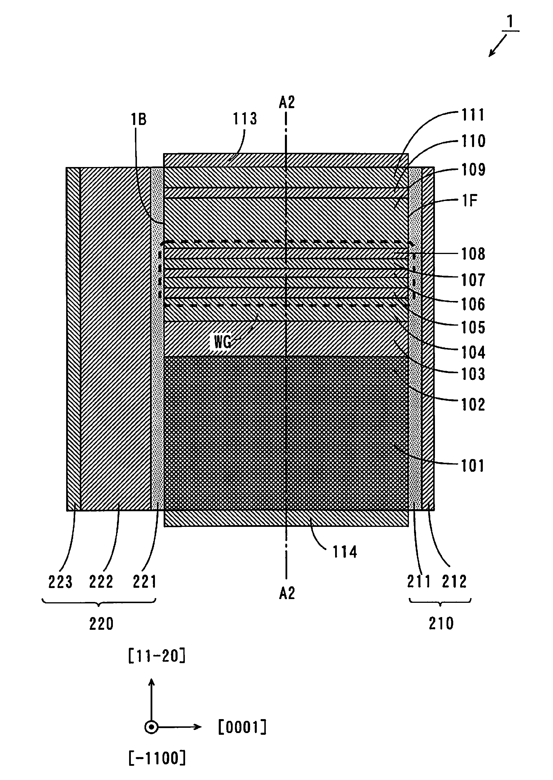
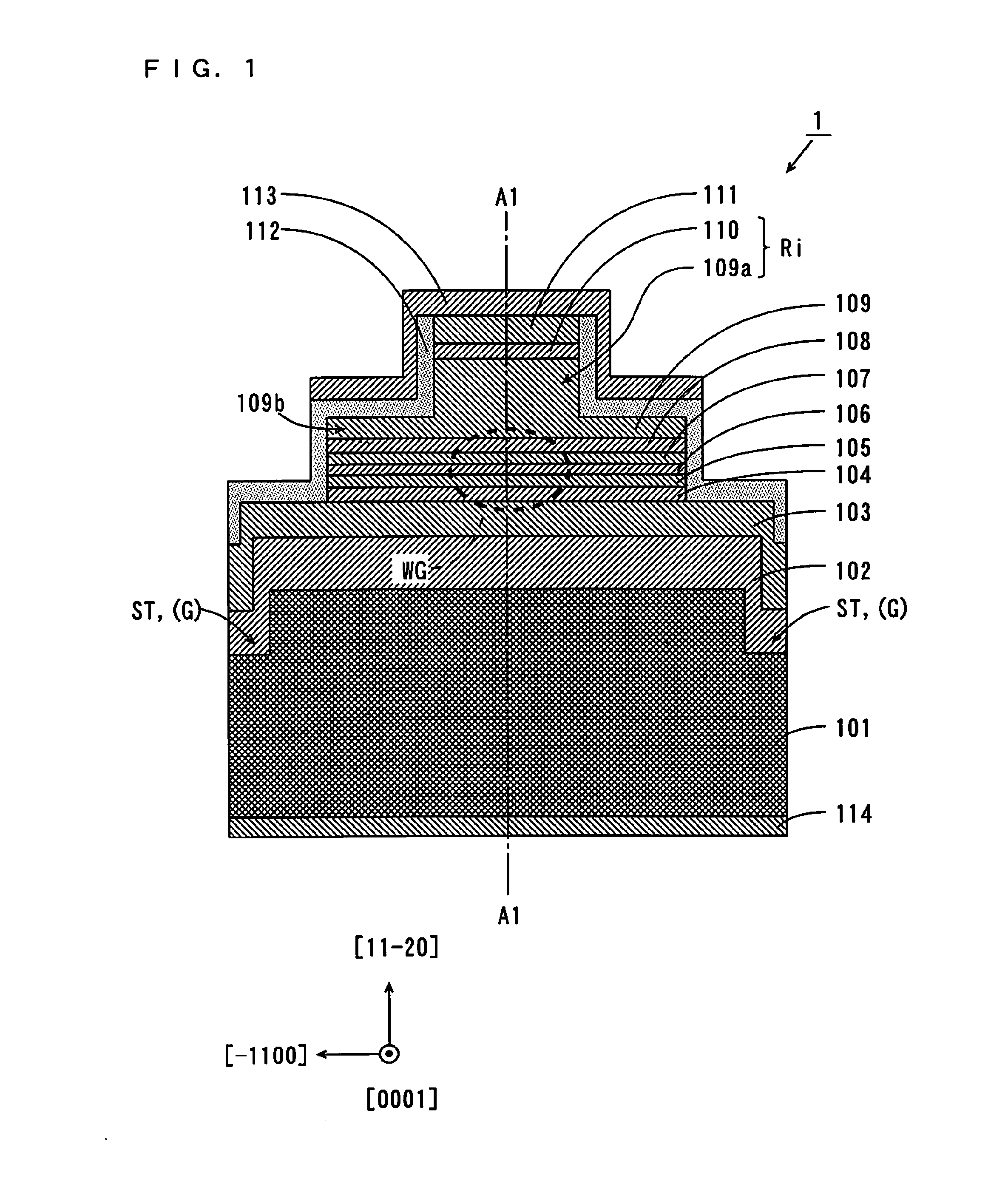
[0039]FIGS. 1 and 2 are vertical sectional views of a nitride based semiconductor laser device according to a first embodiment. A line A1-A1 shown in FIG. 1 represents a position in longitudinal section, and a line A2-A2 shown in FIG. 2 represents a position in longitudinal section.

[0040]As shown in FIGS. 1 and 2, a nitride based semiconductor laser device 1 according to the present embodiment includes an n-type GaN substrate 101 having a thickness of approximately 100 μm in which Si (silicon) has been doped. The carrier concentration of the substrate 101 is approximately 5×1018 cm−3.

[0041]The substrate 101 is an off substrate having a crystal growth plane inclined at approximately 0.3 degrees in a [000 1] direction from a (11 20) plane. As shown in FIG. 1, a pair of steps ST extending in a [0001] direction is formed on an upper surface of the substrate 101. The pair of steps ST is positioned on bo...

second embodiment

2. Second Embodiment

[0090]As to a nitride based semiconductor laser device according to a second embodiment, the difference from the nitride based semiconductor laser device 1 according to the first embodiment will be described.

[0091]FIG. 5 is a vertical sectional view of the nitride based semiconductor laser device according to the second embodiment. In FIG. 5, a vertical section of the nitride based semiconductor laser device 1 along a [0001] direction is shown, similarly to the vertical section shown in FIG. 2 in the first embodiment. A vertical section taken along a line A2-A2 shown in FIG. 5 is the same as the vertical section of the nitride based semiconductor laser device 1 shown in FIG. 1.

[0092]A first dielectric multilayer film 210 is formed on a light emission facet 1F of the nitride based semiconductor laser device 1. The first dielectric multilayer film 210 has a structure in which an AlOXNY film (X>Y) 211a and an Al2O3 film 212a are laminated in this order. Here, the re...

third embodiment

3. Third Embodiment

[0096]As to a nitride based semiconductor laser device according to a third embodiment, the difference from the nitride based semiconductor laser device 1 according to the first embodiment will be described.

[0097]FIG. 6 is a vertical sectional view of the nitride based semiconductor laser device according to the third embodiment. In FIG. 6, a vertical section of the nitride based semiconductor laser device 1 along a [0001] direction is shown, similarly to the vertical section shown in FIG. 2 in the first embodiment. A vertical section taken along a line A2-A2 shown in FIG. 6 is the same as the vertical section of the nitride based semiconductor laser device 1 shown in FIG. 1.

[0098]A first dielectric multilayer film 210 is formed on a light emission facet 1F of the nitride based semiconductor laser device 1. The first dielectric multilayer film 210 has a structure in which an Al2O3 film 211b, an AlOXNY film (X212b, and an Al2O3 film 213b are laminated in this order...


PUM


Abstract

One facet and the other facet of a nitride based semiconductor laser device are respectively composed of a cleavage plane of (0001) and a cleavage plane of (000 1). Thus, the one facet and the other facet are respectively a Ga polar plane and an N polar plane. A portion of the one facet and a portion of the other facet, which are positioned in an optical waveguide, constitute a pair of cavity facets. A first protective film including oxygen as a constituent element is formed on the one facet. A second protective film including nitrogen as a constituent element is formed on the other facet.

Description

BACKGROUND OF THE INVENTION[0001]1. Field of the Invention[0002]The present invention relates to a nitride based semiconductor laser device having a nitride based semiconductor layer.[0003]2. Description of the Background Art[0004]In recent years, nitride-based semiconductor laser devices have been utilized as light sources for next-generation large-capacity disks and have been actively developed.[0005]In such nitride-based semiconductor laser devices, the plane directions of main surfaces of active layers are taken as substantial (H, K, —H—K, O) planes such as (11 20) planes or (1 100) planes, so that piezoelectric fields generated in the active layers can be reduced. As a result, it is known that the luminous efficiency of laser light can be improved. Here, H and K, described above, are any integers, and at least one of H and K is an integer other than zero.[0006]Furthermore, it has been known that the gains of the nitride based semiconductor laser devices can be improved by setti...

Claims


Application Information

Patent Timeline
IPC IPC(8): H01S5/00
CPCH01S5/0282H01S5/0287H01S5/1082H01S2301/176H01S5/3202H01S5/32341H01S5/227H01S5/320225H01S5/2201
Inventor KAMEYAMA, SHINGONOMURA, YASUHIKOHIROYAMA, RYOJIHATA, MASAYUKI
Owner SANYO ELECTRIC CO LTD
Why Eureka
Try Eureka