

Component for semiconductor processing apparatus and manufacturing method thereof
a semiconductor processing and manufacturing method technology, applied in the direction of transportation and packaging, molten spray coating, coating, etc., can solve the problems of high manufacturing cost of semiconductor manufacturing apparatus, high cost of components, and cost increase of conventional components of this kind, so as to achieve cost and durability. the effect of cos
- Summary
- Abstract
- Description
- Claims
- Application Information
AI Technical Summary
Benefits of technology
Problems solved by technology
Method used
Image

Examples
first embodiment
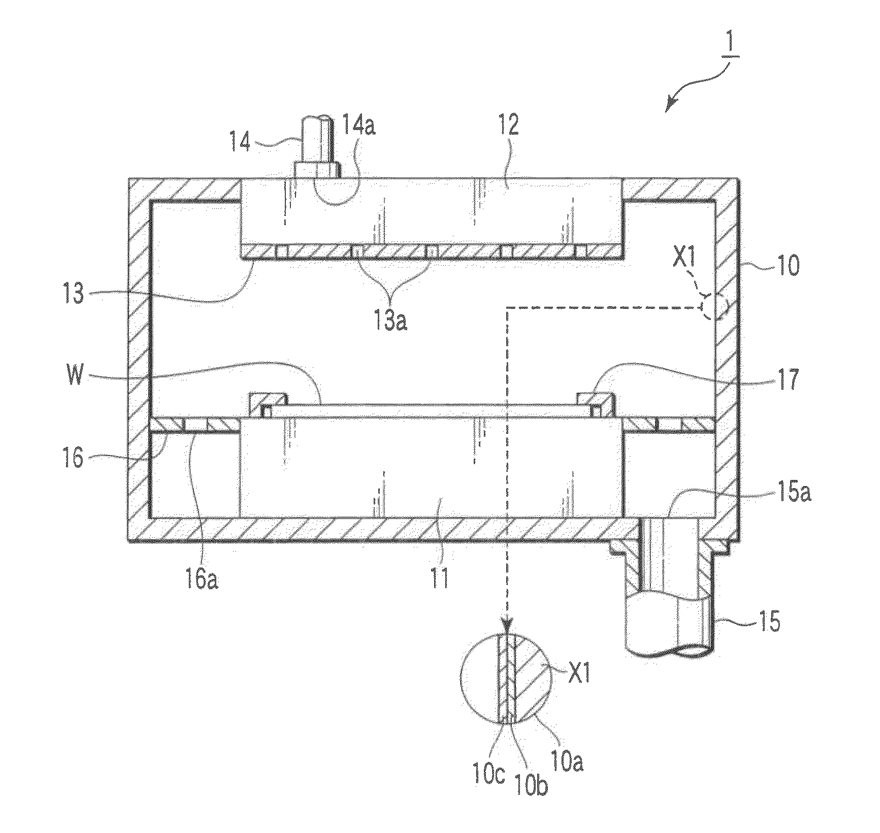
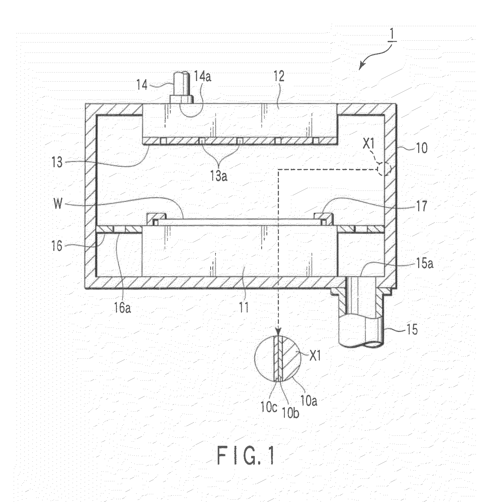
[0060]FIG. 1 is a sectional view showing a semiconductor manufacturing apparatus (semiconductor processing apparatus) according to a first embodiment of the present invention. At first, a brief explanation will be given of components used in the semiconductor manufacturing apparatus, which can be set as surface preparation target objects, with reference to the apparatus shown in FIG. 1. In this apparatus, a wafer W is placed on a worktable 11 located inside a process container 10. A gas supply portion (gas showerhead) 12 is disposed to face the worktable 11 inside the process container 10. The showerhead 12 includes a bottom member 13 with a number of gas holes 13a formed therein, through which a process gas of, e.g., a corrosive gas, is supplied onto the wafer W on the worktable 11. The process gas is supplied from a process gas supply line 14 through the gas supply portion 12 into the process container 10. Gas inside the process container 10 is exhausted by exhaust means (not show...
second embodiment
[0124]FIG. 9 is a view schematically showing steps of a process for manufacturing an environment-proof member (component) according to a second embodiment of the present invention. In FIG. 9,(a) to (d) are views schematically showing a cross-section of a matrix 101 with a film formed on the surface, in the respective steps. According to this embodiment, a surface roughening process is performed on the matrix 101 (FIG. 9,(a)) to be processed by a surface preparation, so that the specific surface area of the matrix is increased (FIG. 9,(b)). Then, an intermediate layer (protection film) F2 is formed (FIG. 9,(c)), and a thermal spray material is thermally sprayed onto the surface of the intermediate layer F2 to form a ceramic thermal spray film F1 (FIG. 9,(d)).
[0125]The material of the matrix 101 is selected from metal materials, such as aluminum and stainless steel, in accordance with the intended use and process recipe of a component. For example, the surface roughening process appli...
third embodiment
[0163]According to a third embodiment, after a semiconductor processing apparatus is assembled, first and second source gases for forming an ALD film are supplied to perform an ALD process on an area where a corrosive gas flows through. Consequently, an ALD film (protection film) is formed on the surface of a metal component that comes in contact with a corrosive gas within an area where a corrosive gas flows through, so at to improve the corrosion resistance of the component relative to the corrosive gas. Examples of the semiconductor manufacturing apparatus encompass not only an apparatus for manufacturing semiconductor devices but also an apparatus for manufacturing flat panel displays. The semiconductor manufacturing apparatus may be an apparatus arranged to use a corrosive gas as a process gas, an apparatus arranged to supply a corrosive gas used as a cleaning gas into a process container to perform cleaning for the interior of the process container after a substrate process, o...
PUM
| Property | Measurement | Unit |
|---|---|---|
| thickness | aaaaa | aaaaa |
| porosity | aaaaa | aaaaa |
| thickness | aaaaa | aaaaa |
Abstract
Description
Claims
Application Information