Deposition processes for titanium nitride barrier and aluminum

a technology of titanium nitride and aluminum, which is applied in the direction of resistive material coating, plasma technique, solid-state devices, etc., can solve the problems of increasing resistivity, affecting other material layers, and degrading the resulting integrated circuit, so as to increase the nitrogen gas flow and reduce the dc power

Inactive Publication Date: 2009-04-02
APPLIED MATERIALS INC
View PDF99 Cites 273 Cited by
  • Summary
  • Abstract
  • Description
  • Claims
  • Application Information

AI Technical Summary

Benefits of technology

[0010]Embodiments described herein provide a method for forming two titanium nitride materials by different PVD processes, such that a metallic titanium nitride layer is initially formed and a titanium nitride retarding layer is formed over a portion of the metallic titanium nitride layer. The metallic titanium nitride layer is deposited by a PVD process conducted in metallic mode, while the titanium nitride retarding layer is deposited by a PVD process conducted in poison mode by increasing the nitrogen gas flow and decreasing the DC power applied to the titanium target relative to the metallic mode. Subsequently, an aluminum seed layer may be selectively deposited on exposed portions of the metallic titanium nitride layer by a CVD process. Thereafter, an aluminum bulk layer may be deposited on exposed portions of the aluminum seed layer and the titanium nitride retarding layer during an aluminum PVD process.

Problems solved by technology

For the current submicron generation of semiconductor devices, any microscopic reaction at an interface between interconnection layers can cause degradation of the resulting integrated circuits (e.g., increase the resistivity of the interconnection layers).
However, CVD or ALD processes may require high deposition temperatures (e.g., >600° C.) to form a typical titanium nitride layer, which may affect other material layers that are in contact with the metal nitride barrier layers.
At high temperatures dopants in the semiconductor junctions may diffuse out of the buried junctions, potentially changing the characteristics thereof.
Additionally, when chlorine-based chemistries are used to form the metal nitride barrier layers during a CVD or ALD process, such nitride layers typically contain chlorine contaminants therein.
A high chlorine concentration is undesirable because chlorine may migrate from the metal nitride barrier layer into adjacent material layers (e.g., interconnection layers) which can increase the contact resistance of such layers, potentially changing the characteristics of integrated circuits made therefrom.
However, the metal nitride barrier layers formed from an organometallic precursor often contain high levels of carbon, which increases the resistivity of the material.
Other problems that occur while manufacturing electronic devices is due to the need for smaller structures, especially for apertures and vias, which are approaching widths of 0.12 μm and smaller.
These high aspect ratio structures have complicated surfaces to deposit barrier layers on, and also small vias that need to be filled with conductive materials, such as aluminum.
The reliability of an aluminum plug is lost if gaps are formed within the vias while being filled with aluminum.

Method used


Image

  • Deposition processes for titanium nitride barrier and aluminum
  • Deposition processes for titanium nitride barrier and aluminum
  • Deposition processes for titanium nitride barrier and aluminum

Examples


Embodiment Construction

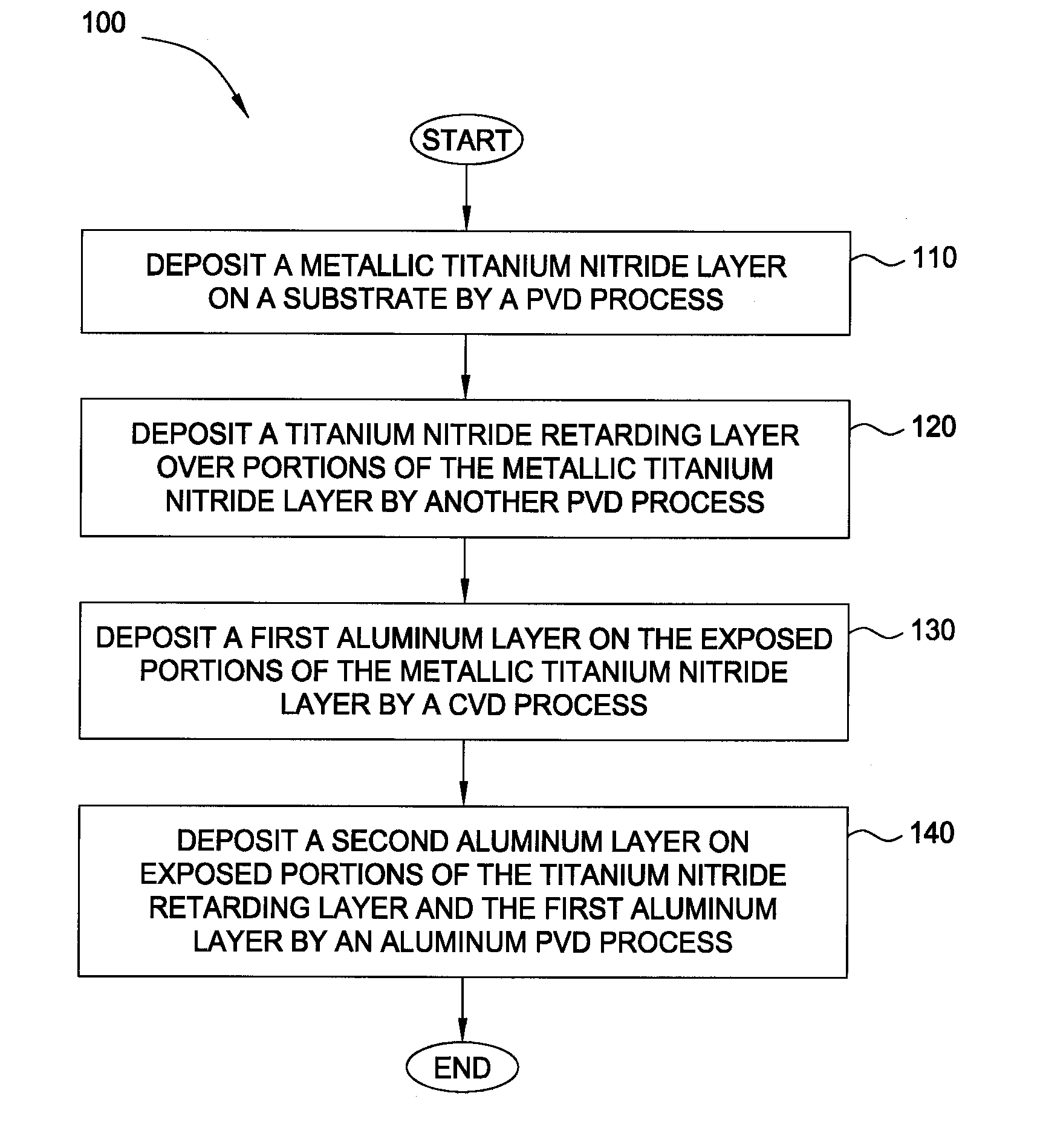
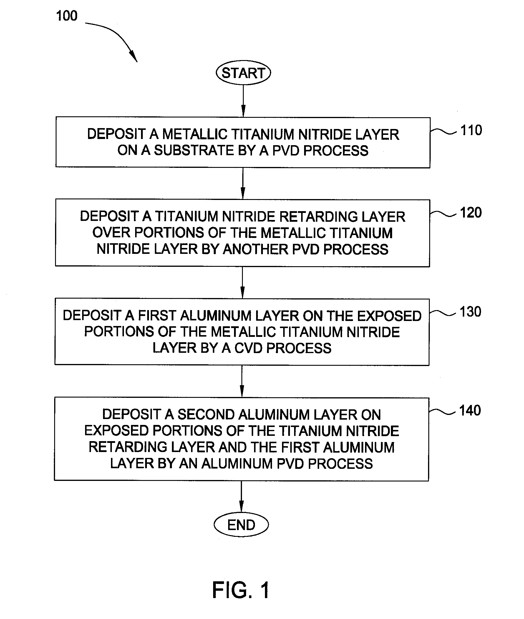
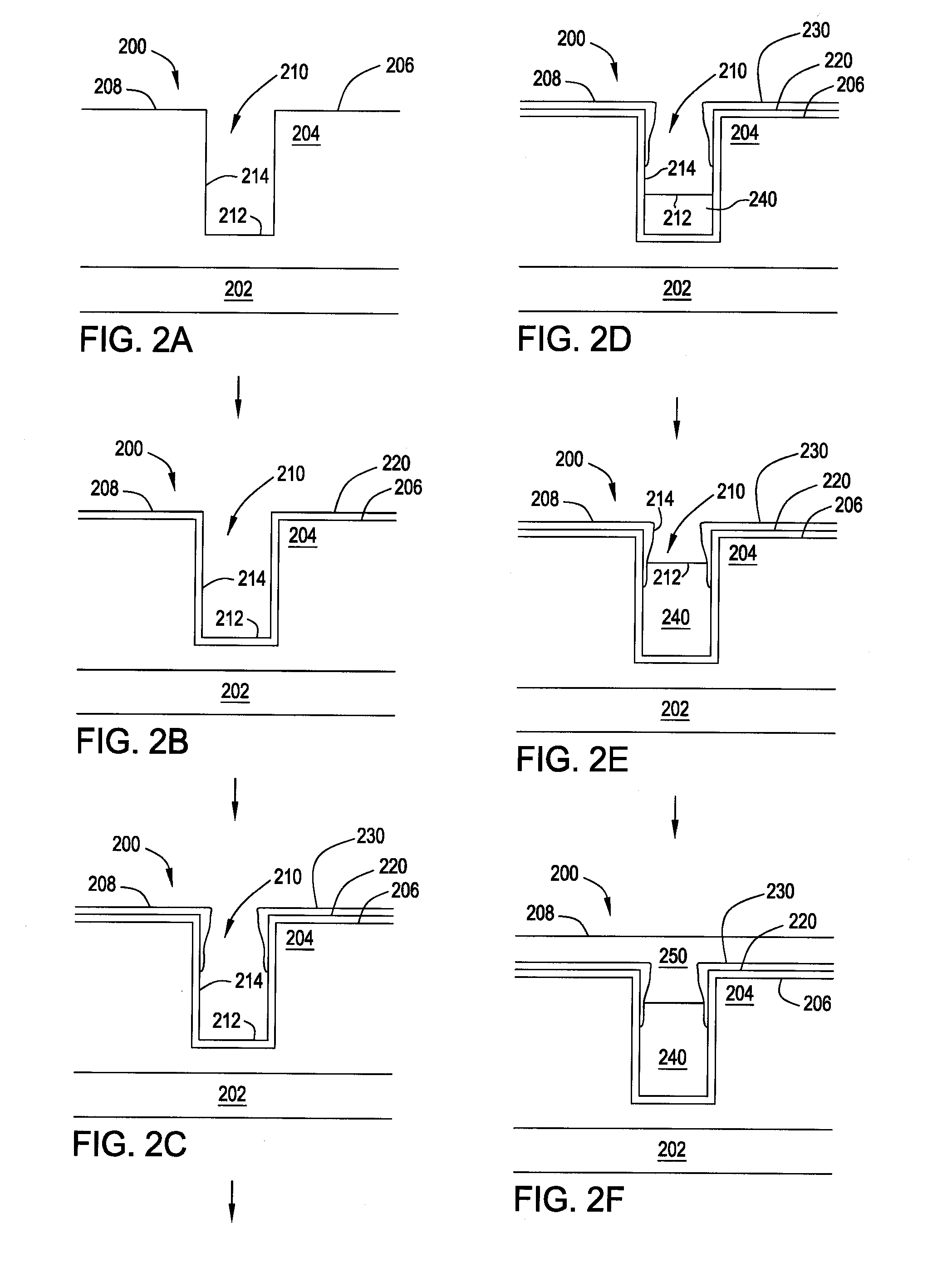
[0029]Embodiments described herein provide a method for forming two titanium nitride materials by different PVD processes, such that a metallic titanium nitride layer is initially formed on a substrate and a titanium nitride retarding layer is formed over at least a portion of the metallic titanium nitride layer. The titanium nitride retarding layer is primarily deposited across the field of the substrate and minimally deposited, if at all, within any exposed apertures contained on the substrate. Subsequently, an aluminum seed layer may be selectively deposited on exposed portions of the metallic titanium nitride layer by a CVD process, preferably, a MOCVD process. Thereafter, an aluminum bulk layer may be deposited on exposed portions of the aluminum seed layer and the titanium nitride retarding layer during an aluminum PVD process.

[0030]In one embodiment, a method for forming a conductive material on a substrate is provided which includes positioning the substrate within a process...


PUM

PropertyMeasurementUnit
poweraaaaaaaaaa
poweraaaaaaaaaa
poweraaaaaaaaaa

Abstract

Embodiments described herein provide a method for forming two titanium nitride materials by different PVD processes, such that a metallic titanium nitride layer is initially formed by a PVD process in a metallic mode and a titanium nitride retarding layer is formed over a portion of the metallic titanium nitride layer by a PVD process in a poison mode. Subsequently, a first aluminum layer, such as an aluminum seed layer, may be selectively deposited on exposed portions of the metallic titanium nitride layer by a CVD process. Thereafter, a second aluminum layer, such as an aluminum bulk layer, may be deposited on exposed portions of the first aluminum layer and the titanium nitride retarding layer during an aluminum PVD process.

Description

BACKGROUND OF THE INVENTION[0001]1Field of the Invention[0002]Embodiments of the invention generally relate to the formation of metal nitride barrier layers and conductive metal layers deposited thereon, and more particularly, to titanium nitride barrier layers and aluminum layers deposited thereon.[0003]2. Description of the Related Art[0004]In the manufacture of integrated circuits, barrier layers are often used to inhibit the diffusion of metals and other impurities into regions underlying such barrier layers. These underlying regions may include transistor gates, capacitor dielectric, semiconductor substrates, metal lines, as well as many other structures that appear in integrated circuits. For the current submicron generation of semiconductor devices, any microscopic reaction at an interface between interconnection layers can cause degradation of the resulting integrated circuits (e.g., increase the resistivity of the interconnection layers). Consequently, barrier layers have b...

Claims


Application Information

Patent Timeline
Patent Type & Authority Applications(United States)
IPC IPC(8): H05H1/24
CPCC23C14/0036C23C14/0089C23C14/0641H01J37/32449H01J37/32706H01J37/34H01L23/53223H01L21/28556H01L21/32051H01L21/76831H01L21/76843H01L21/76876H01L21/76879H01L21/2855H01L2924/0002H01L2924/00
Inventor LEE, WEI TIWANG, YEN-CHIHHASSAN, MOHD FADZLI ANWARKIM, RYEUN KWANPARK, HYUNG CHULGUO, TEDRITCHIE, ALAN A.
Owner APPLIED MATERIALS INC
Why Eureka
Try Eureka