Methods for producing improved epitaxial materials

a technology of epitaxial materials and epitaxial layers, applied in the direction of basic electric elements, electrical equipment, semiconductor devices, etc., to achieve the effects of simplifying the elo process, reducing the density of surface defects, and increasing the probability of defects

Active Publication Date: 2009-04-09
S O I TEC SILICON ON INSULATOR THECHNOLOGIES +1
View PDF18 Cites 34 Cited by
  • Summary
  • Abstract
  • Description
  • Claims
  • Application Information

AI Technical Summary

Benefits of technology

The invention provides a method for producing a planar film with reduced surface defects compared to a film grown directly on a support substrate. By using a patterned mask, defects are reduced through coalescence and annihilation of dislocations that have originated at the substrate interface and propagated into the growing material. This method simplifies the process and reduces the level of defects in the material.

Problems solved by technology

The patent text discusses the challenges in preparing high-quality layers of semiconductor materials, especially compound materials like gallium nitride and other Group III nitrides. These materials have low crystal quality and are difficult to grow on suitable substrates, which results in a high density of defects and dislocations. The text highlights the need for improved methods to produce better quality layers of these materials for use in various applications.

Method used


Image

  • Methods for producing improved epitaxial materials
  • Methods for producing improved epitaxial materials
  • Methods for producing improved epitaxial materials

Examples


examples

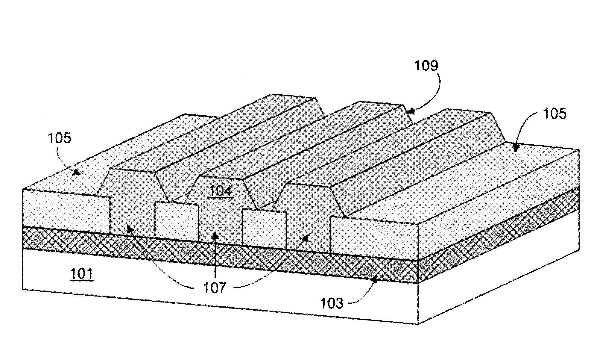
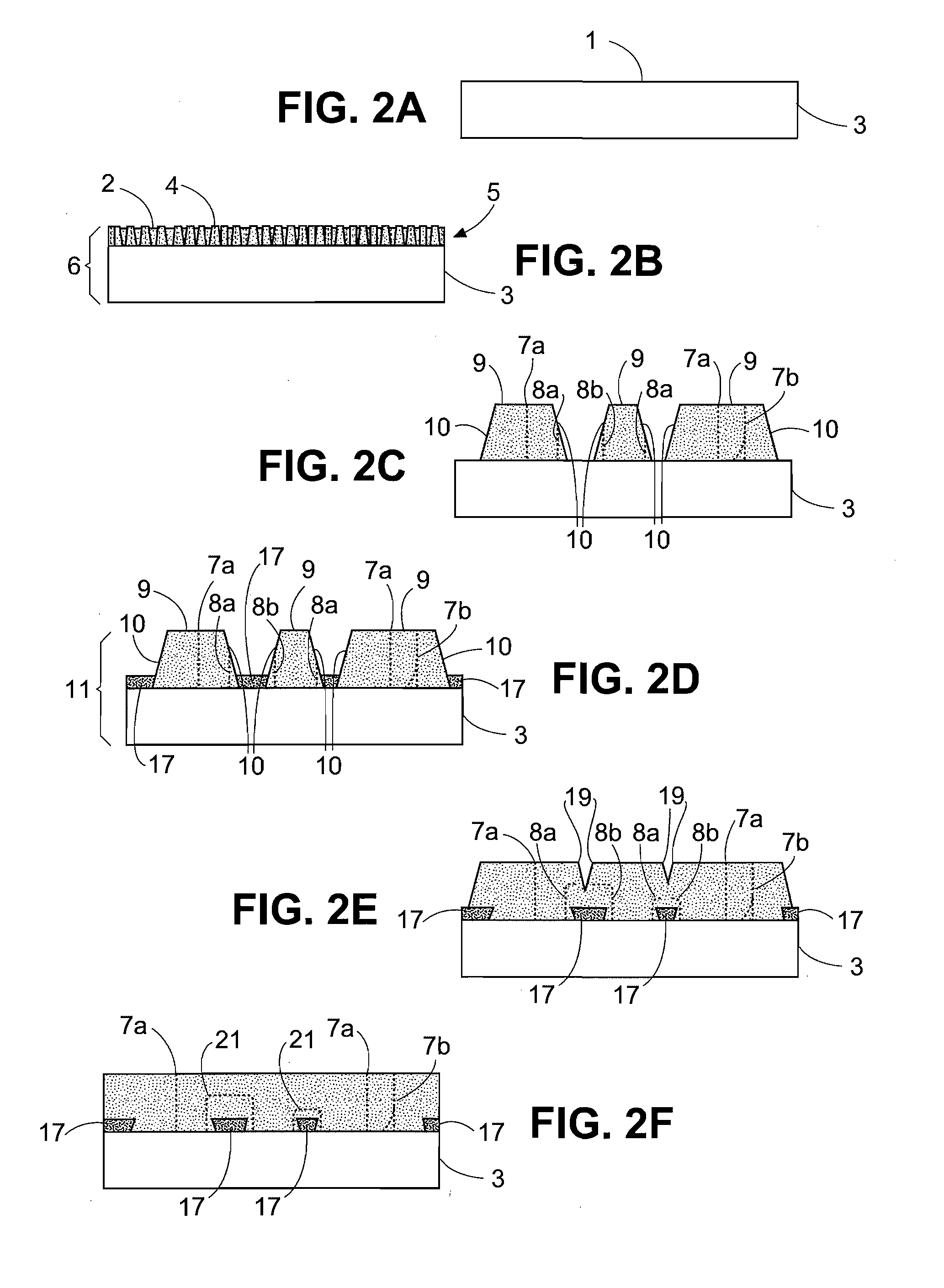
[0067]FIG. 4 illustrates an example of a gallium nitride sample grown by the methods described above. FIG. 4. demonstrates a transmission electron micrograph (TEM) imaged from a cross-section sample of a gallium nitride crystal grown on (0001) sapphire substrate with diffraction condition g=. The sapphire substrate is shown at the bottom of the image 403 and the plurality of dark lines in the image corresponds to defects in the GaN crystal. Defect structures 402 are unaffected by the introduction of the dielectric layer and therefore likely correspond to defect structures 7 in FIG. 2e. However, the defect structures 401 exhibit a change in propagation direction, as with defect structures 8 in FIG. 2e and are therefore more likely to interact with other defects, resulting in defect annihilation / coalescence and a subsequent reduction in defect density. The reduction in defect density made possible via the methods of this invention can be again be evaluated via FIG. 4. Examination of t...


PUM


Abstract

This invention provides methods for fabricating substantially continuous layers of group III nitride semiconductor materials having low defect densities. The methods include epitaxial growth of nucleation layers on a base substrate, thermally treatment of said nucleation layer and epitaxial growth of a discontinuous masking layer. The methods outlined promote defect reduction through masking, annihilation and coalescence, therefore producing semiconductor structures with low defect densities. The invention can be applied to a wide range of semiconductor materials, both elemental semiconductors, e.g., combinations of Si (silicon) with strained Si (sSi) and/or Ge (germanium), and compound semiconductors, e.g., group II-VI and group III-V compound semiconductor materials.

Description


Claims


Application Information

Patent Timeline
Owner S O I TEC SILICON ON INSULATOR THECHNOLOGIES
Why Eureka
Try Eureka