Semiconductor device, method of manufacturing the same, and semiconductor substrate

a semiconductor substrate and semiconductor technology, applied in semiconductor devices, semiconductor/solid-state device details, electrical devices, etc., can solve the problems of increasing contamination in molding dies, uneven backside of semiconductor substrates, defective appearances, etc., to reduce the number of steps in the manufacturing process, eliminate defective appearances of products, and increase the resistance to cracks and exfoliation of packages

Inactive Publication Date: 2009-04-09
PANASONIC CORP
View PDF4 Cites 9 Cited by
  • Summary
  • Abstract
  • Description
  • Claims
  • Application Information

AI Technical Summary

Benefits of technology

[0018]As described above, according to the present invention, the molding resin has a larger thickness on the edge of the semiconductor device than on a portion around the center of the semiconductor device, so that the molding resin clamps the semiconductor substrate from the edge to the center. Consequently, it is possible to increase a resistance to a crack and exfoliation of a package.
[0019]Thus even when a semiconductor device is manufactured by collective molding, it is possible to eliminate a defective appearance of a product and reduce the number of steps in a manufacturing process to suppress an increase in the cost of the product while preventing a crack and exfoliation of the package to improve the reliability of the product.

Problems solved by technology

Further, the back side of the semiconductor substrate may have an uneven surface because of a warp occurring over the substrate, a wiring pattern formed on the back side to connect external electrode terminals, and so on.
When such a gap occurs, resin burrs may occur on the back side of the semiconductor substrate during resin molding, cause a defective appearance, and increase contamination in the molding dies.
In some cases, the productivity may be reduced by lower yields and an increased number of steps, so that a product may become less reliable and the cost may increase.

Method used


Image

  • Semiconductor device, method of manufacturing the same, and semiconductor substrate
  • Semiconductor device, method of manufacturing the same, and semiconductor substrate
  • Semiconductor device, method of manufacturing the same, and semiconductor substrate

Examples


Embodiment Construction

[0040]A semiconductor device, a method of manufacturing the same, and a semiconductor substrate according to an embodiment of the present invention will be specifically described below with reference to the accompanying drawings.

FIRST STRUCTURAL EXAMPLE OF THE SEMICONDUCTOR DEVICE

[0041]First, a first structural example of the semiconductor device according to the embodiment of the present invention will now be described.

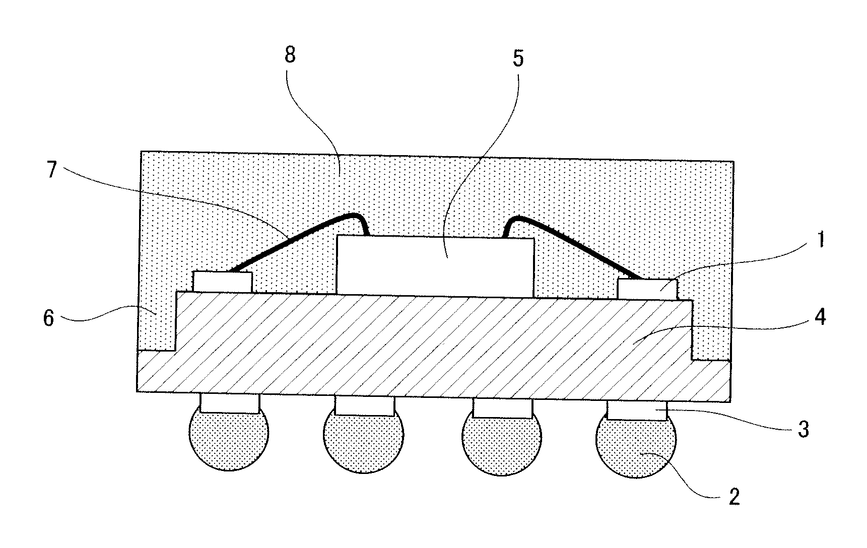
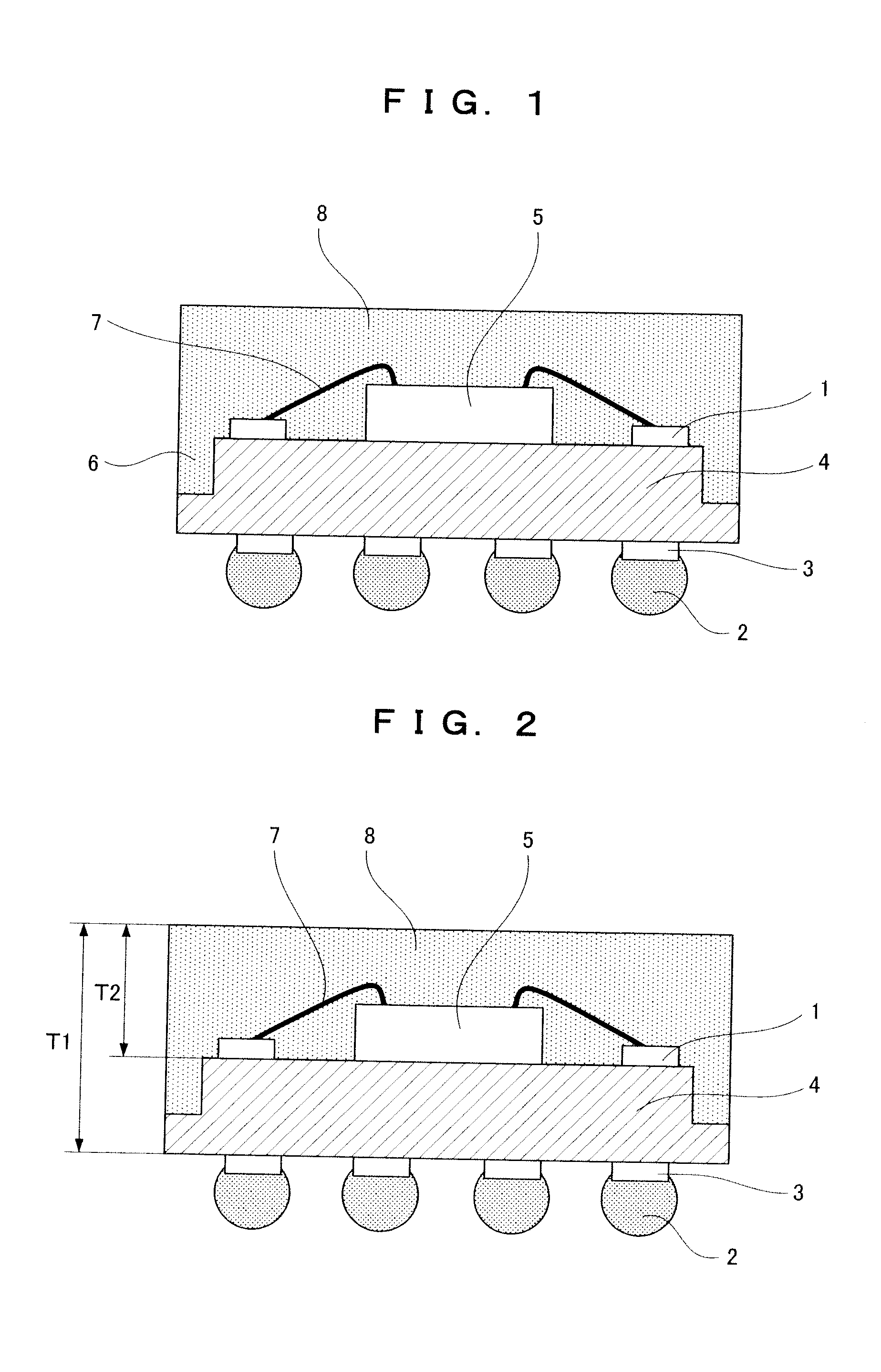
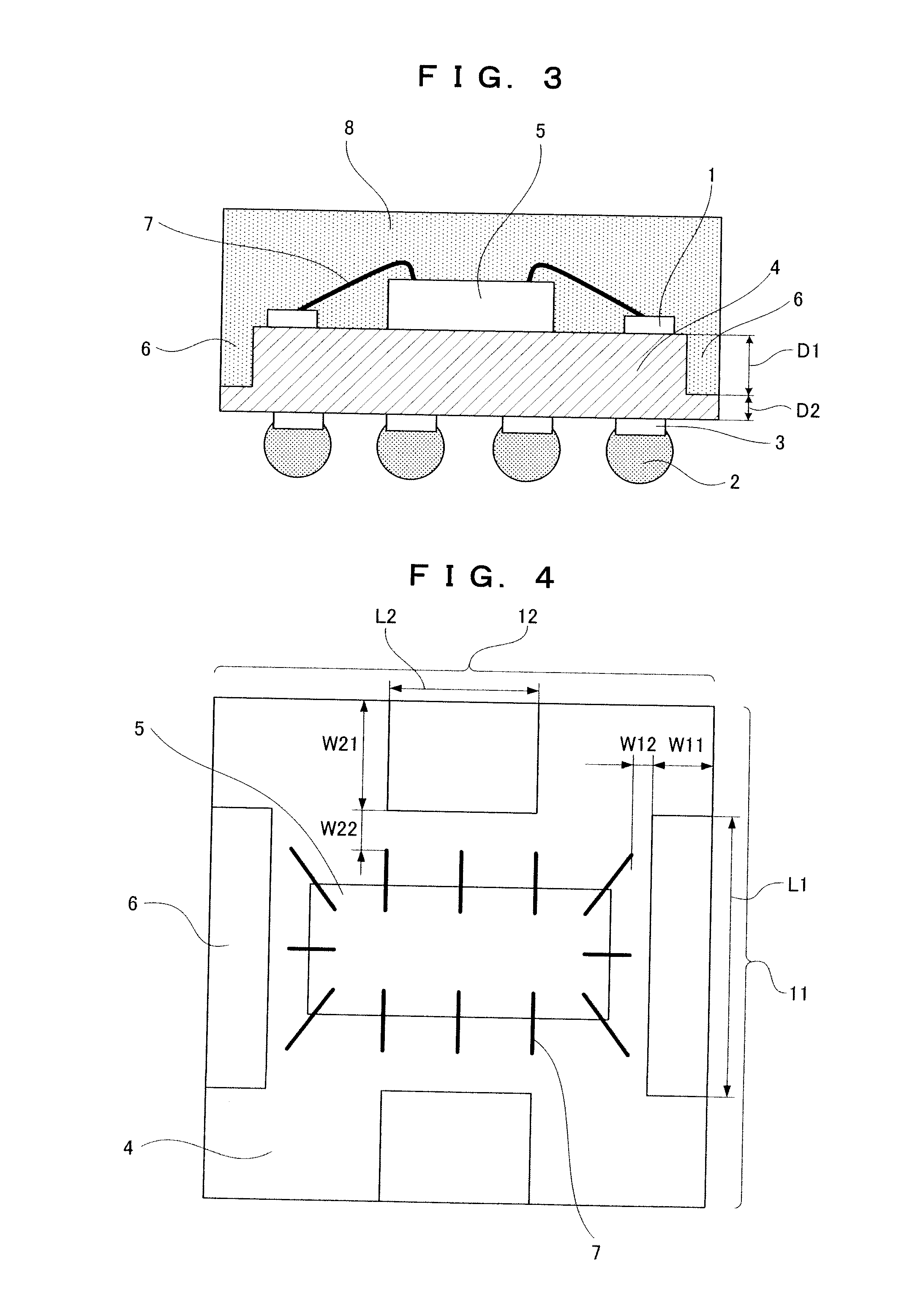
[0042]FIG. 1 is a sectional view showing the first structural example of the semiconductor device according to the present embodiment. In the illustrated semiconductor device, as shown in FIG. 1, first electrodes 1 are formed on the front side of a semiconductor substrate 4, second electrodes 3 are formed on the back side of the semiconductor substrate 4, and recessed portions 6 are formed on the edge of the front side of the semiconductor substrate 4. Further, a semiconductor element 5 having a plurality of electrodes (not shown) for external connection is formed o...


PUM


Abstract

According to the present invention, for collective molding of semiconductor devices, a semiconductor substrate includes first electrodes formed on the front side, second electrodes formed on the back side and connected to external electrode terminals, and a plurality of semiconductor element mounting regions 203. Along partition lines 202 for partitioning the semiconductor substrate into the plurality of semiconductor element mounting regions 203, recessed portions 205 are formed on the partition lines 202 on the front side of the semiconductor substrate.

Description

FIELD OF THE INVENTION [0001]The present invention relates to a semiconductor device manufactured by collective molding, a method of manufacturing the same, and a semiconductor substrate for the collective molding of the semiconductor device.BACKGROUND OF THE INVENTION [0002]Conventionally, in a typical resin molded semiconductor device, a semiconductor element is mounted on a substrate made of resin and is molded with thermosetting resin while being set in molding dies. Further, a surface of the substrate on which the semiconductor element is mounted is molded with resin, that is, only one surface of the substrate is molded with resin.[0003]Moreover, in order to efficiently produce semiconductor devices by collective molding used as resin molding, a semiconductor substrate is divided along predetermined partition lines after resin molding. Thus desired semiconductor devices can be obtained in the same production facilities.[0004]In a conventional semiconductor device (e.g., see Jap...

Claims


Application Information

Patent Timeline
Patent Type & Authority Applications(United States)
IPC IPC(8): H01L23/48H01L21/00
CPCH01L2225/06517H01L2924/01015H01L2924/01033H01L2924/01006H01L2924/01005H01L24/49H01L2225/0651H01L2224/97H01L2224/49175H01L2224/49171H01L2224/48227H01L2224/48091H01L2224/45144H01L2224/16145H01L25/0657H01L2924/01079H01L2924/10158H01L2924/15153H01L2924/15165H01L2924/15311H01L2924/18301H01L21/561H01L23/3107H01L23/562H01L24/45H01L24/48H01L24/94H01L24/97H01L25/0652H01L2924/00014H01L2224/85H01L2924/00H01L2924/181H01L2924/15159H01L2924/15162H01L2924/00012
Inventor AKAHOSHI, TOSHITAKA
Owner PANASONIC CORP
Why Eureka
Try Eureka