Wafer container with staggered wall structure

Active Publication Date: 2009-04-16
DAEWON SEMICON PACKAGING INDAL
View PDF18 Cites 42 Cited by
  • Summary
  • Abstract
  • Description
  • Claims
  • Application Information

AI Technical Summary

Benefits of technology

[0008]Yet another embodiment of the invention concerns a cover for a wafer container that engages to a ba

Problems solved by technology

Semiconductor wafers are fragile substrates that can easily become scratched or damaged if not properly protected during transport.
Frequently, the top and bottom half of wafer containers are improperly combined by an operator or become misaligned by forces that impact the containers during shipping.
Such misalignment may contamin

Method used


Image

  • Wafer container with staggered wall structure
  • Wafer container with staggered wall structure
  • Wafer container with staggered wall structure

Examples


Embodiment Construction

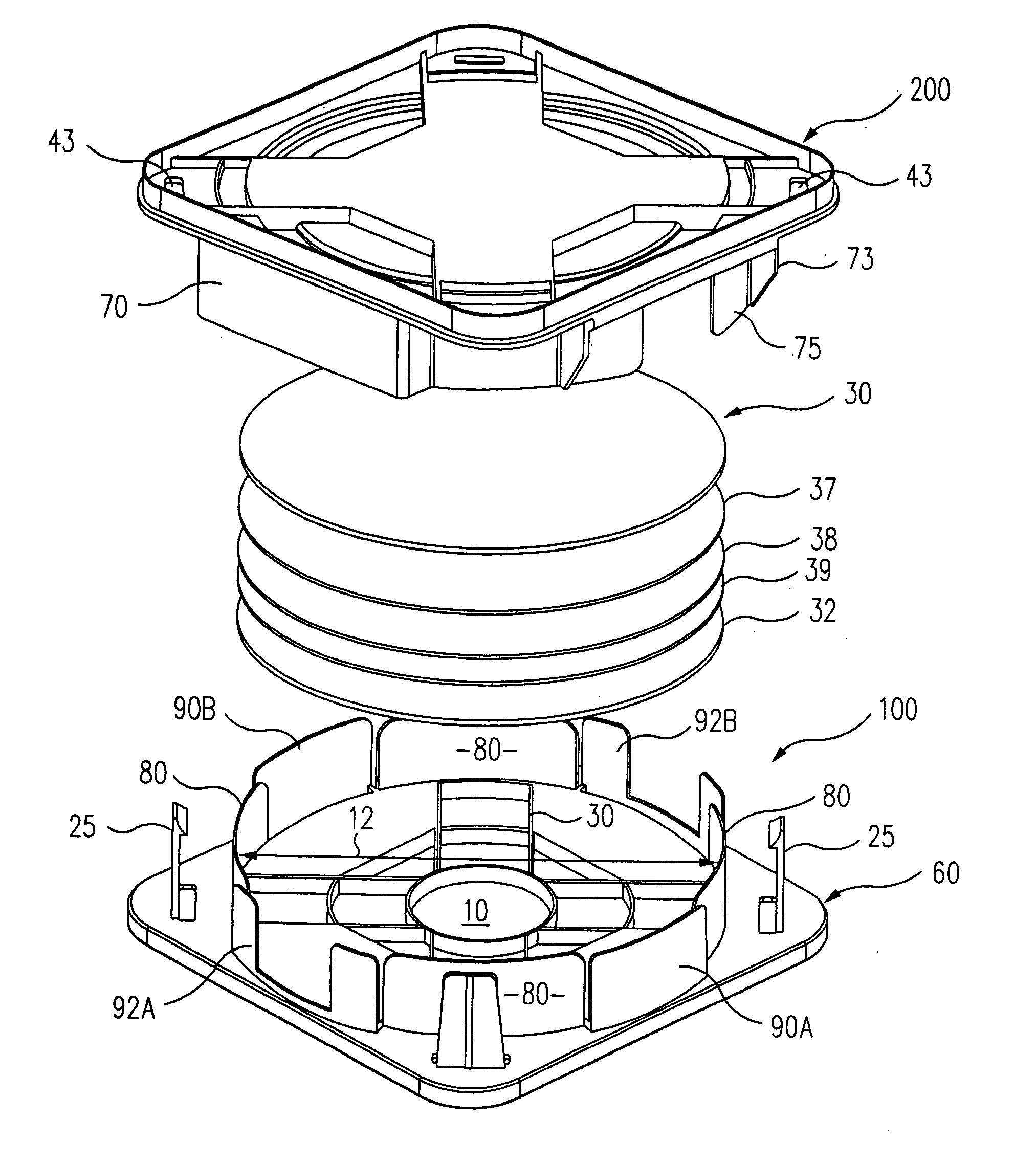
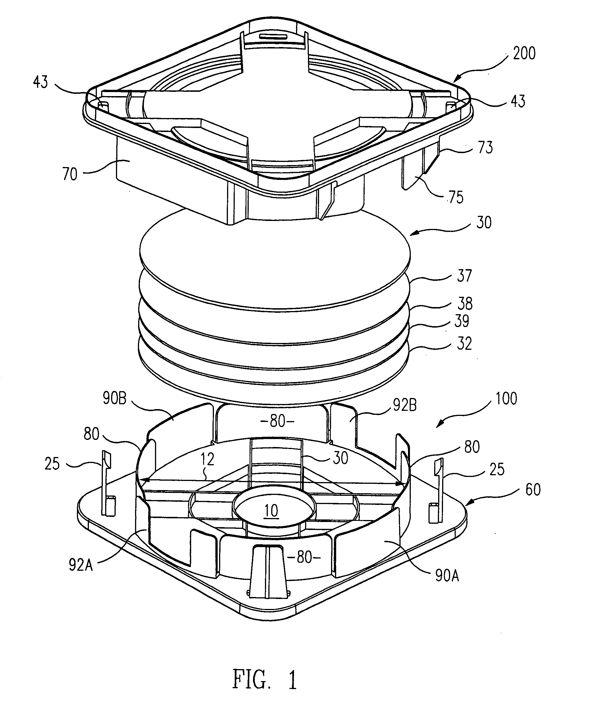
[0024]The container of the present invention stores semiconductor wafers, or semiconductor film frames. FIG. 1 illustrates the two halves of the container, a base 100 and its corresponding cover 200. A ribbed pattern 30 on the floor 10 of deck 60 serves to reinforce the integrity of base 100. The storage area of base 100 is defined by inner walls 80, floor 10, and outer walls 90A, 90B, 92A, and 92B. Interposed between cover 200 and base 100 are wafers 30, 32 and wafer separators 37-39.

[0025]Upon impact, outer wall segments 90A, 90B, 92A, and 92B will flex to the inner diameter 12 of inner wall segments 80. Outer wall segments 90A, 90B, 92A, and 92B absorb the bulk of energy from side impact, thereby transferring a reduced amount of energy to the inner wall segments 80. Consequently, wafers 30 and 32 are sheltered from the brunt of forceful impact by the staggered wall structure of the invention.

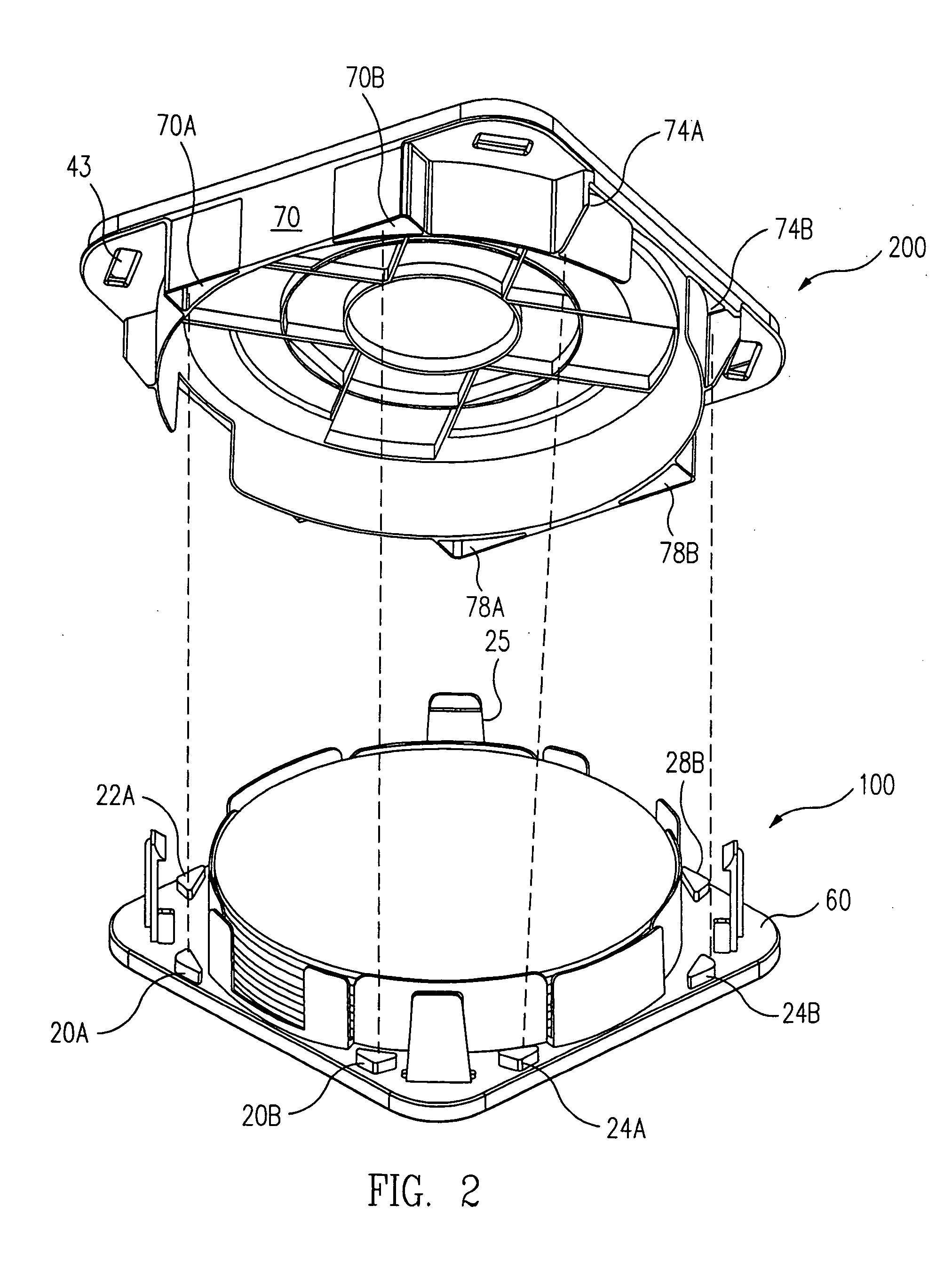
[0026]FIG. 2 illustrates an alternative embodiment for the base 100 of wafer container 25...


PUM


Abstract

A wafer container comprising a base and a cover that nest together. The base includes a staggered wall structure composed of inner and outer walls. The staggered wall structure is arranged so that forces from side impacts are absorbed principally by outer wall segments. A rib on the cover restrains the outer wall segments from flexing beyond the inner wall diameter. Reference tabs on the base facilitate alignment of the base to the cover.

Description

BACKGROUND OF THE INVENTION[0001]Semiconductor wafers are fragile substrates that can easily become scratched or damaged if not properly protected during transport. Each semiconductor wafer is patterned with numerous integrated circuits on a silicon substrate. Numerous containers have been developed to protect semiconductor wafers from damage during shipping and handling.[0002]Frequently, the top and bottom half of wafer containers are improperly combined by an operator or become misaligned by forces that impact the containers during shipping. Such misalignment may contaminate, crack, or otherwise damage the valuable wafers stored within the containers.[0003]Among the variety of horizontal wafer containers for semiconductor wafers, are containers having a dual wall structure. U.S. Pat. No. 6,193,068 (Lewis) is one example. The double walls in Lewis were designed to protect wafers from forces that may contact the outer wall of the base. However, in Lewis the outer wall is directly be...

Claims


Application Information

Patent Timeline
IPC IPC(8): B65D85/00
CPCH01L21/67369H01L21/67386H01L21/67379H01L21/67373
Inventor PYLANT, JAMES D.HOFFMAN, GALEN J.WABER, ALANAVERY, AMOS E.
Owner DAEWON SEMICON PACKAGING INDAL
Why Eureka
Try Eureka