Liquid crystal display device and method of manufacturing the same
- Summary
- Abstract
- Description
- Claims
- Application Information
AI Technical Summary
Benefits of technology
Problems solved by technology
Method used
Image
Examples
first embodiment
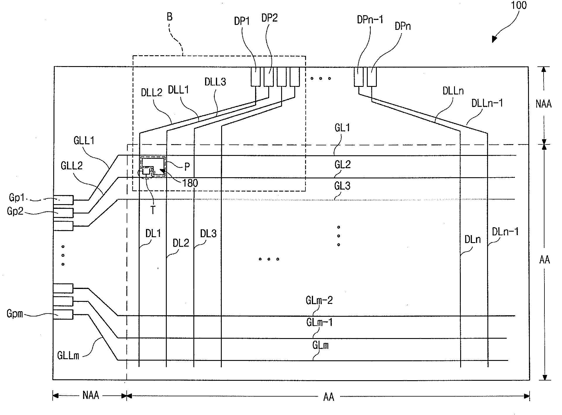
[0037]FIG. 3 is a plan view illustrating an array substrate of an LCD device according to the present invention.
[0038]Referring to FIG. 3, the array substrate includes a display region AA to display images and a non-display region NAA.
[0039]In the display region AA, the array substrate includes first to mth gate lines GL1 to GLm each extended in a first direction and first to nth data lines DL1 to DLn each extended in a second direction and crossing the first to mth gate lines GL1 to GLm to define a plurality of pixel regions P in a matrix form.
[0040]A thin film transistor T is located in each pixel region P and connected to the corresponding gate and data lines. A pixel electrode 180 is located in each pixel region P and connected to the thin film transistor T. The pixel electrode 180 may be formed of a transparent conductive material including indium-tin-oxide (ITO), indium-zinc-oxide (IZO) and indium-tin-zinc-oxide (ITZO). When the LCD device is an in-plane switching mode LCD dev...
third embodiment
[0077]In the array substrate it is explained that the odd data link line 350a and the odd data pad electrode 360a are formed at the same layer as the gate line 320a and 320b, and the even data link line 350b and the even data pad electrode 360b are formed at the same layer as the data line 330a and 330b. Alternatively, the odd data link line 350a and the odd data pad electrode 360a may be formed at the same layer as the data line 330a and 330b, and the even data link line 350b and the even data pad electrode 360b are formed at the same layer as the gate line 320a and 320b.
[0078]As described in the embodiments of the present invention, since the odd and even data link lines are formed at different layers with the gate insulating layer therebetween, short-circuit between the even and odd data link lines can be prevented, and the data link region and the non-display region can be minimized. Further, since the bridge patterns are used, the resistance difference between the metal lines...
PUM
 Abstract
Description
Claims
Application Information


