Phase-change random access memory device, system having the same, and associated methods
a random access memory and phase-change technology, applied in the field of phase-change random access memory devices, a system having the same, can solve the problems of increasing the time required to perform the discharge operation, inaccurate subsequent write operation of the first cell, and unsatisfactory voltage in the first bit lin
- Summary
- Abstract
- Description
- Claims
- Application Information
AI Technical Summary
Benefits of technology
Problems solved by technology
Method used
Image


Examples
first embodiment
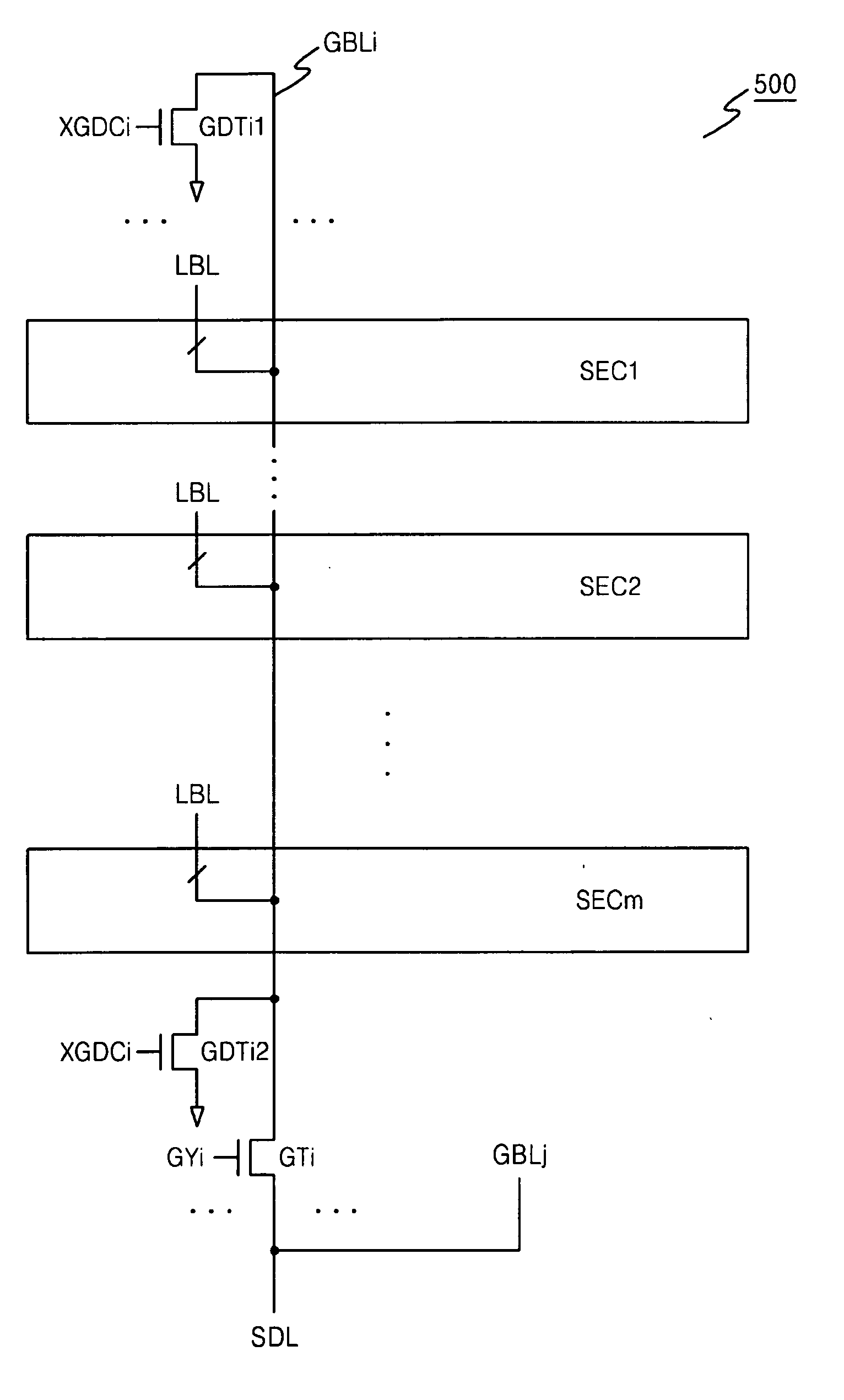
[0057]FIG. 5 illustrates a circuit diagram of a PRAM device 500 according to a
[0058]Referring to FIG. 5, a global bit line GBLi of the PRAM device 500 may include a plurality of first discharge units, e.g., GDTi1 and GDTi2, which respond to a first discharge signal XGDCi to discharge the global bit line GBLi connected thereto. A jth global bit line GBLj (not shown in FIG. 5) may have the same structure as the ith global bit line GBLi.
[0059]In an implementation, the PRAM device 500 may have two first discharge units GDTi1 and GDTi2 for the global bit line GBLi. The two first discharge units GDTi1 and GDTi2 for the global bit line GBL may be disposed at respective ends of the global bit line GBL. In an implementation, GDTi1 and GDTi2 may each include metal oxide semiconductor (MOS) transistors, the gates of which may be controlled by a first discharge signal XGDCi. One end of each MOS transistor may be connected to a ground voltage line. In an implementation, as shown in FIG. 5, the f...
second embodiment
[0062]FIG. 6 illustrates a circuit diagram of a PRAM device 600 according to a
[0063]Referring to FIG. 6, a first discharge unit GDTi of a global bit line GBLi of a PRAM device 600 may be disposed between two sectors. For example, for a plurality of sectors, i.e., a first sector to an mth sector (where m is a positive integer equal to or greater than 2) shared by a plurality of global bit lines GBLi and GBLj, the first discharge unit GDTi may be disposed between an xth sector SECx and a (x+1)th sector SECx+1, wherein x is a positive integer less than m. The first discharge unit GDTi may be, e.g., an NMOS transistor, which may have a gate controlled by the first discharge signal to discharge the corresponding global bit line GBLi in the manner described above in connection with FIG. 5.
[0064]The first discharge unit GDTi may be disposed at the center of the global bit lines GBLi. For example, for the case that m is a multiple of 2, the first discharge unit GDTi may be disposed between ...
third embodiment
[0066]FIGS. 7 and 8 illustrate circuit diagrams of PRAM devices 700 and 800 according to a
[0067]Referring to FIGS. 7 and 8, local bit lines LBL1 to LBLn of the PRAM devices 700 and 800 may include a plurality of second discharge units LDT11, LDT12, LDTn1 and LDTn2, which may respond to corresponding second discharge signals XLDC1 to XLDCn to discharge the connected local bit lines LBL1 to LBLn. The PRAM devices 700 and 800 may include two second discharge units for each local bit lines, e.g., at respective ends of the corresponding local bit lines, as shown in FIGS. 7 and 8.
[0068]The PRAM devices 700 and 800 may each include a plurality of sub cell arrays SCA. The sub cell arrays SCA may be disposed between second discharge units LDTn1 and LDTn2 on opposite ends of the corresponding local bit lines LBL1 to LBLn, as shown in FIGS. 7 and 8.
[0069]The second discharge units LDT11, LDT12, LDTn1 and LDTn2 may each include a MOS transistor, the gate of which may be controlled by correspond...
PUM
 Abstract
Description
Claims
Application Information
 - R&D
- Intellectual Property
- Life Sciences
- Materials
- Tech Scout
- Unparalleled Data Quality
- Higher Quality Content
- 60% Fewer Hallucinations
Browse by: Latest US Patents, China's latest patents, Technical Efficacy Thesaurus, Application Domain, Technology Topic, Popular Technical Reports.
© 2025 PatSnap. All rights reserved.Legal|Privacy policy|Modern Slavery Act Transparency Statement|Sitemap|About US| Contact US: help@patsnap.com