Systems, methods, and apparatus for multilayer superconducting printed circuit boards

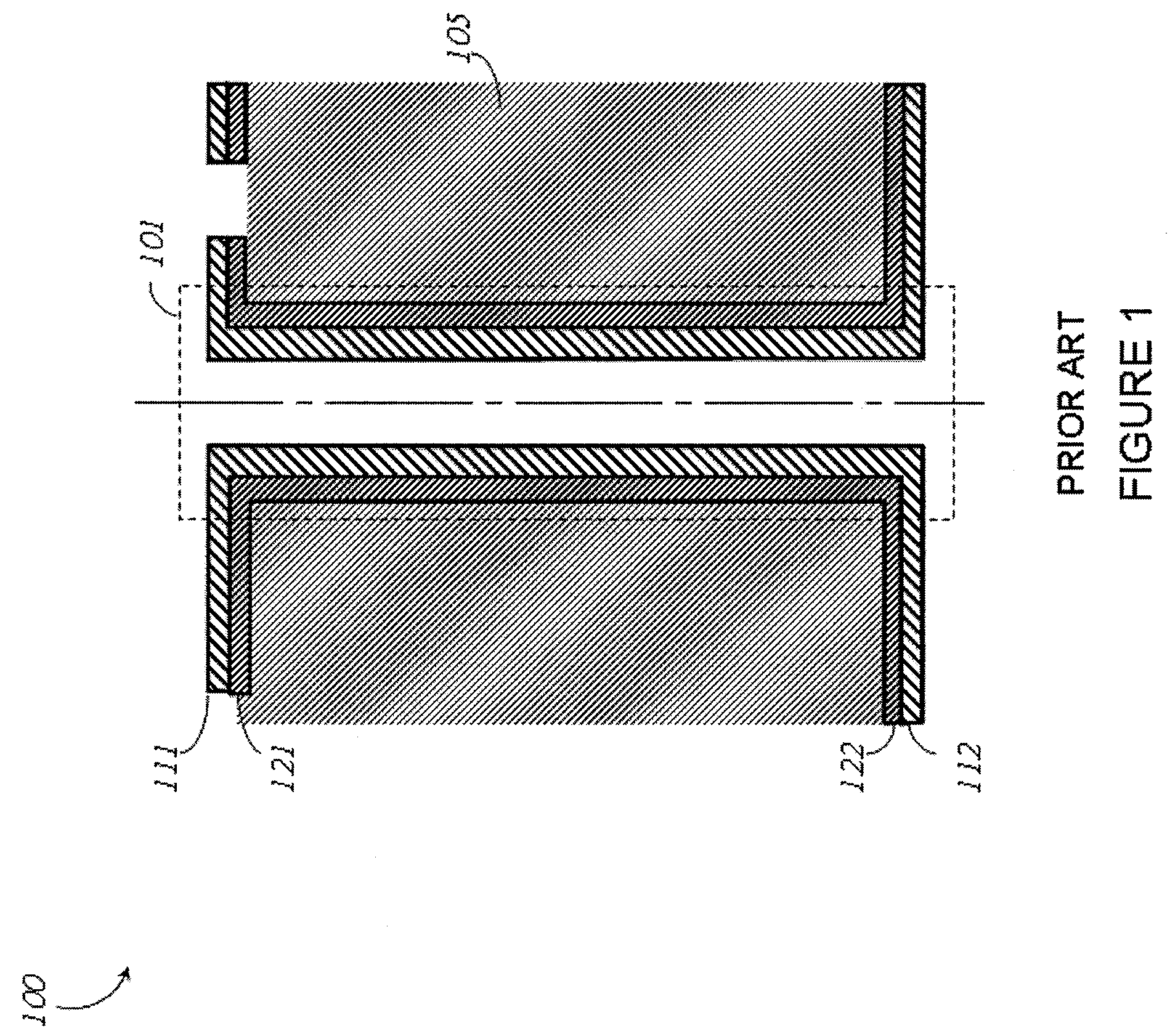
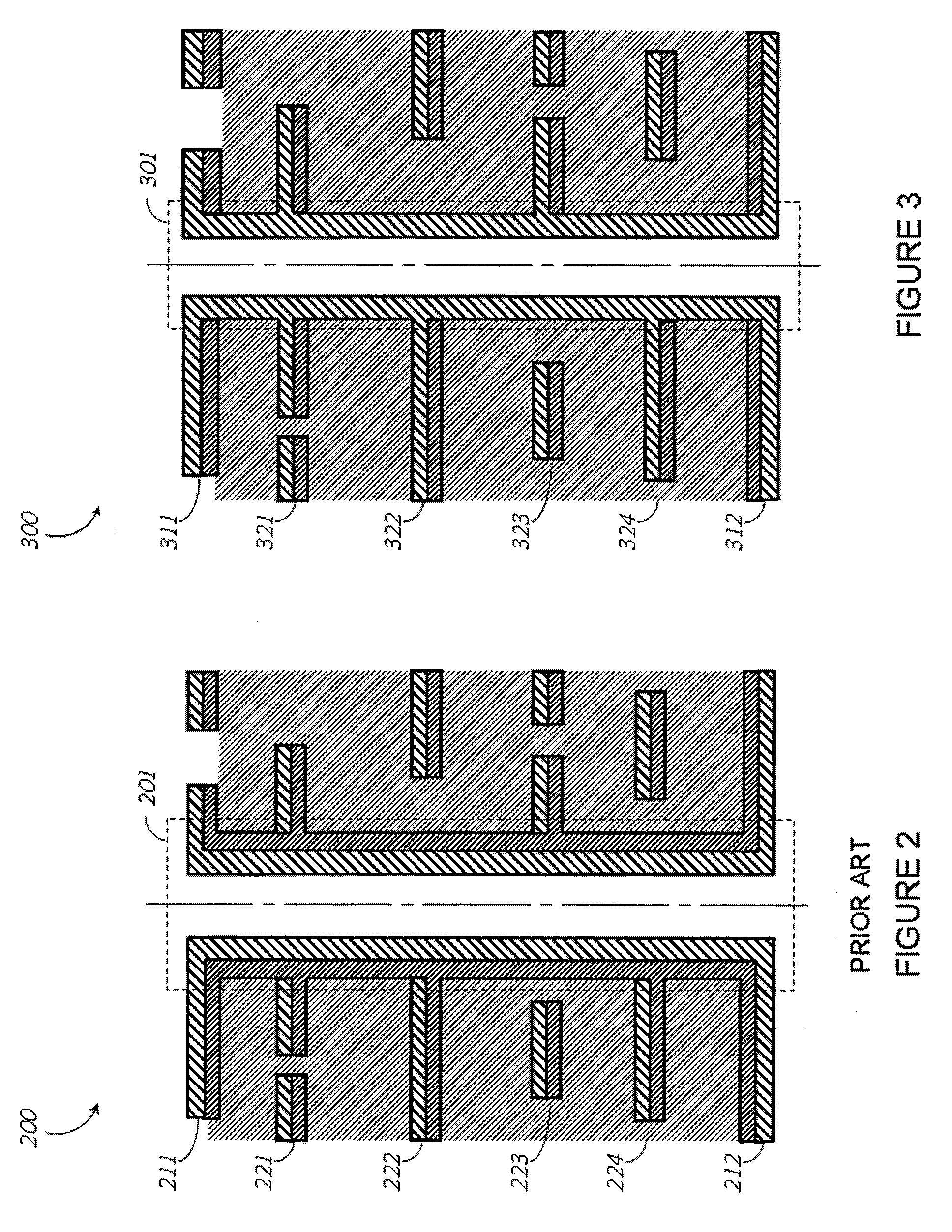
a printed circuit board and superconducting technology, applied in the manufacture/treatment of superconductor devices, permanent superconductor devices, superconducting magnets/coils, etc., can solve the problems of limiting the capabilities of non-superconducting pcb technology, and the sophistication of superconducting circuits to date has been limited to simple single- or double-layer pcbs

Active Publication Date: 2009-04-16
D WAVE SYSTEMS INC
View PDF8 Cites 37 Cited by
  • Summary
  • Abstract
  • Description
  • Claims
  • Application Information

AI Technical Summary

Benefits of technology

[0008]The first superconducting current path may be carried on the first surface of the first insulative substrate layer. The first surface of the first insulative substrate layer may be a first outer surface physically accessible from an exterior of the superconducting printed circuit board. The second superconducting current path may be carried on the second surface of the first insulative substrate layer. The second superconducting current path may be carried on the first surface of the second insulative substrate layer and the first surface of the second insulative substrate layer may be successively adjacent the second surface of the first insulative substrate layer. The superconducting printed circuit board may further include a fourth superconducting current path positioned to be on a second surface side of the second electrically insulative substrate layer; and a fifth superconducting current path that extends through the second electrically insulative substrate layer and superconductingly couples the fourth superconducting current path with at least one of the first and the second superconducting current paths. The first surface of the first insulative substrate layer may be a first outer surface physically accessible from an exterior of the superconducting printed circuit board and the second surface of the second electrically insulative substrate layer may be a second outer surface physically accessible from the exterior of the superconducting printed circuit board. The superconducting printed circuit board may further include at least a third electrically insulative substrate layer having a first surface and a second surface opposed to the first surface, the third electrically insulative substrate layer physically coupled to the second electrically insulative substrate layer; at least one additional superconducting current path carried by the second surface of the third electrically insulative substrate layer; and a sixth superconducting current path that extends through the third electrically insulative substrate layer and superconduct

Problems solved by technology

However, a number of challenges that are inherent in non-superconducting electronics (e.g., power consumption and heat dissipation) continue to influence each stage of development of these devices an

Method used


Image

  • Systems, methods, and apparatus for multilayer superconducting printed circuit boards
  • Systems, methods, and apparatus for multilayer superconducting printed circuit boards
  • Systems, methods, and apparatus for multilayer superconducting printed circuit boards

Examples


Embodiment Construction

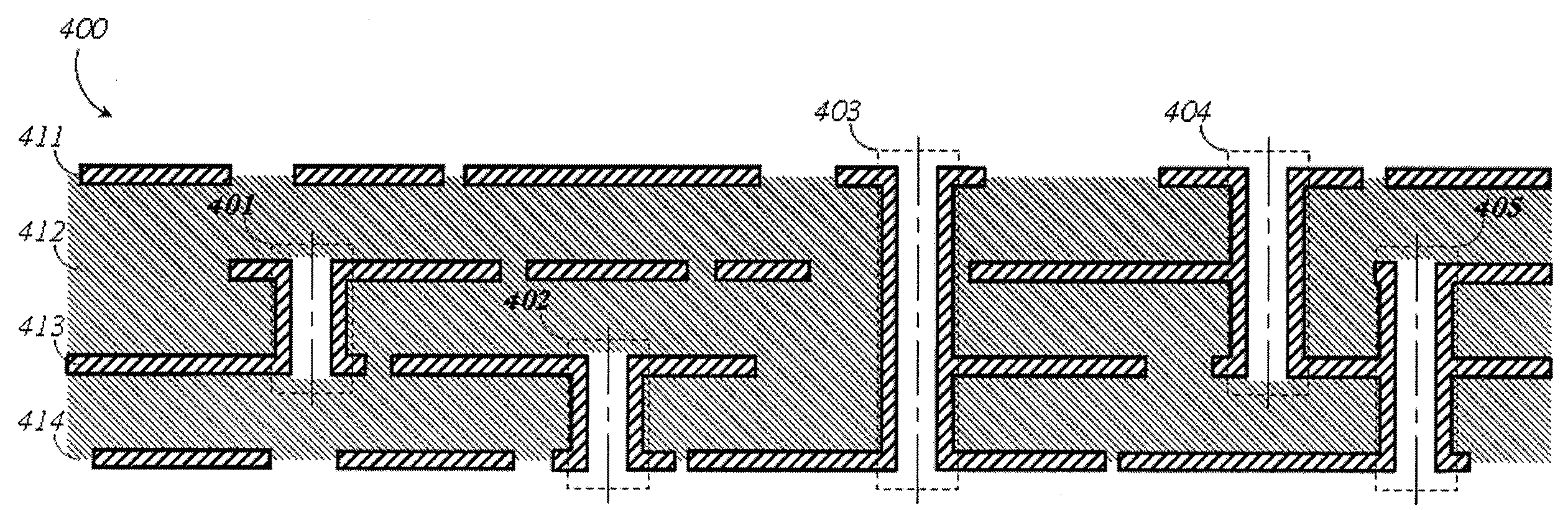
[0017]In the following description, certain specific details are set forth in order to provide a thorough understanding of various disclosed embodiments. However, one skilled in the relevant art will recognize that embodiments may be practiced without one or more of these specific details, or with other methods, components, materials, etc. In other instances, well-known structures associated with printed circuit boards, superconducting circuits, devices and control systems including microprocessors and drive circuitry have not been shown or described in detail to avoid unnecessarily obscuring descriptions of the embodiments.

[0018]Unless the context requires otherwise, throughout the specification and claims which follow, the word “comprise” and variations thereof, such as, “comprises” and “comprising” are to be construed in an open, inclusive sense, that is as “including, but not limited to.”

[0019]Reference throughout this specification to “one embodiment” or “an embodiment” means t...


PUM

PropertyMeasurementUnit
Currentaaaaaaaaaa
Superconductivityaaaaaaaaaa

Abstract

Superconducting connections are provided to internal layers of a multi-layer circuit board structure, for example by superconducting vias.

Description

CROSS REFERENCE TO RELATED APPLICATIONS[0001]This application claims benefit under 35 U.S.C. 119(e) of U.S. Provisional Patent Application Ser. No. 60 / 979,031, filed Oct. 10, 2007, entitled “Systems, Methods and Apparatus for Multilayer Superconducting Printed Circuit Boards”, which is incorporated herein by reference in its entirety.BACKGROUND[0002]1. Field[0003]The present systems, methods, and apparatus generally relate to the realization of superconducting circuits on multilayer superconducting printed circuit boards.[0004]2. Description of the Related Art[0005]Since they were first introduced around the time of World War II, conventional printed circuit boards (“PCBs”) have simultaneously reduced in size and grown in sophistication. An important step in this evolution was the introduction of conductive vias to provide electrical communication between separate layers of a PCB. In non-superconducting applications, multilayer PCBs (i.e., PCBs with two or more layers of conductive ...

Claims


Application Information

Patent Timeline
IPC IPC(8): H01L39/02H01L39/24H05K1/00H05K3/00
CPCH01L39/14H05K1/09H05K1/115H05K3/24Y10T428/24917H05K2201/0391H05K2201/09627Y10T29/49124H05K3/429H05K1/0298
Inventor UCHAYKIN, SERGEY V.
Owner D WAVE SYSTEMS INC
Why Eureka
Try Eureka