Circuit board structure integrated with semiconductor chip and method of fabricating the same

a semiconductor chip and circuit board technology, applied in the manufacture of printed circuits, printed circuit aspects, basic electric elements, etc., can solve the problems of increasing stencil costs in response to the reduction of pad size and pad pitch, difficult to deposit solder material, and difficult to reduce the thickness of stencils, so as to simplify the integration form of circuit boards and semiconductor chips. , to achieve the effect of preventing flash problems, reducing steps and costs of fabrication processes

Inactive Publication Date: 2007-01-25
PHOENIX PRECISION TECH CORP
View PDF3 Cites 31 Cited by
  • Summary
  • Abstract
  • Description
  • Claims
  • Application Information

AI Technical Summary

Benefits of technology

[0012] Another objective of the present invention is to provide a circuit board structure integrated with semiconductor chip and a method of fabricating the same, to avoid various problems caused by forming electrical connection between a semiconductor chip and a circuit board in the conventional technology.
[0013] Still another objective of the present invention is to provide a circuit board structure integrated with semiconductor chip and a method of fabricating the same, to simplify an integration form of a circuit board and a semiconductor chip so as to reduce steps and costs of fabrication processes.
[0014] A further objective of the present invention is to provide a circuit board structure integrated with semiconductor chip and a method of fabricating the same, to prevent a flash problem caused during a molding process in the conventional technology, so as to effectively improve production quality and product reliability of a semiconductor device.
[0015] In accordance with the above and other objectives, the present invention proposes a method of fabricating a circuit board structure integrated with semiconductor chip, comprising the steps of: providing a supporting plate, which can be a general carrier board or circuit board, wherein the supporting plate is formed with at least one through cavity, such that at lease one semiconductor chip having a plurality of conductive contacts is received in the cavity; and providing an anisotropic conductive film (ACF) layer and a circuit board having a plurality of conductive contacts on a surface thereof, such that the circuit board is pressed and mounted to the supporting plate by the ACF layer pressed therebetween, and the conductive contacts of the circuit board are electrically connected to the conductive contacts of the chip via the ACF layer, so as to form the circuit board structure integrated with semiconductor chip. The conductive contacts of the chip comprise electrode pads and conductive bumps formed on the electrode pads. Further, the chip can also be directly electrically connected to the circuit board by the ACF layer having a plurality of conductive particles therein. As a result, steps and costs of fabrication processes are reduced as compared to conventional electrical connecting technology of forming a plurality of openings in a dielectric layer, performing electroplating to electrically connect circuit layers and so on.
[0016] By the foregoing fabrication meth

Problems solved by technology

This not only causes an alignment problem in subsequently forming pre-solder bumps but also requires reduction in opening size of a stencil for the stencil printing technology, making the solder material difficult to be deposited on the contact pads due to the occupied space and height of the insulating protective layer, such that the yield of stencil printing technology becomes extremely low, and costs of the stencil are increased in response to the reduction in pad size and pad pitch, leading to undesirable raise of the fabrication costs.
This increases steps and costs of the fabrication processes and may also cause the reliability risks during the fabrication processes.
Whether employing the flip-chip packaging technology or wire-bonding packaging technology, fabrication of the circuit board and packaging of the chip both require various fabrication machines and steps, and have complicated fabrication processes and high fabrication costs.
However in practice, the mold is limited by the design of the semiconductor package such that the size of a molding cavity a

Method used


Image

  • Circuit board structure integrated with semiconductor chip and method of fabricating the same
  • Circuit board structure integrated with semiconductor chip and method of fabricating the same
  • Circuit board structure integrated with semiconductor chip and method of fabricating the same

Examples


Embodiment Construction

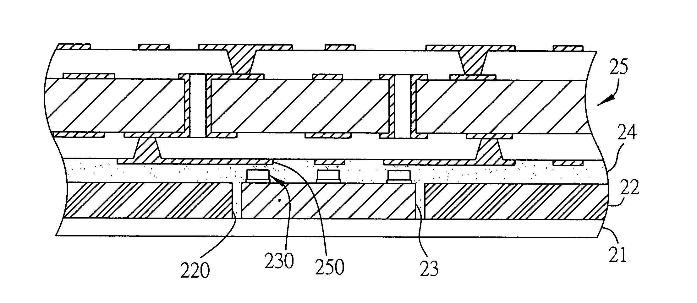
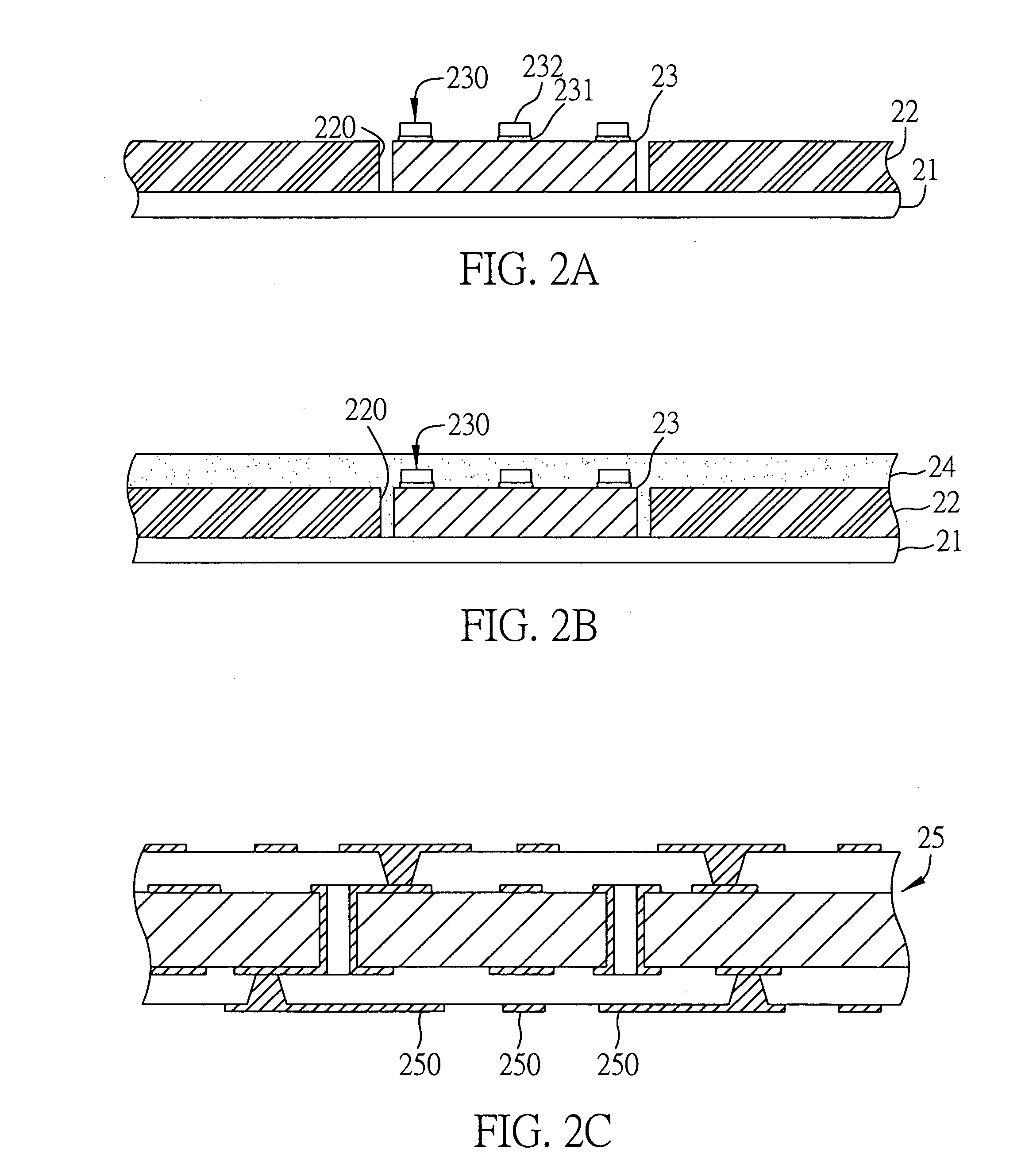
[0021]FIGS. 2A to 2E are cross-sectional schematic diagrams showing steps of a method of fabricating a circuit board structure integrated with semiconductor chip according to the present invention.

[0022] Referring to FIG. 2A, firstly, a supporting plate 22 is provided, which can be a carrier board such as a metallic plate, insulating plate, etc. or even a circuit board, and the supporting plate 22 is formed with at least one through cavity 220. A carrier 21 can be formed on a side of the supporting plate 22 to seal a side of the cavity 220. The carrier 21 may be an adhesive layer, such that at least one semiconductor chip 23 may be mounted via a surface thereof on the carrier 21 and received in the cavity 220 of the supporting plate 22, wherein conductive contacts 230 on an active surface of the semiconductor chip 23 are exposed from the cavity 220 of the supporting plate 22. The conductive contacts 230 of the semiconductor chip 23 comprise electrode pads 231 formed on the semicond...


PUM


Abstract

A circuit board structure integrated with semiconductor chip and a method of fabricating the same are proposed. A supporting plate formed with at least one cavity is provided and a semiconductor chip having a plurality of conductive contacts is embedded in the cavity. An anisotropic conductive film (ACF) layer and a circuit board formed with a plurality of conductive contacts on a surface thereof are provided. The circuit board is pressed to the supporting plate by the ACF layer, wherein the conductive contacts of the circuit board are electrically connected to the conductive contacts of the chip via the ACF layer, so as to form the circuit board structure integrated with semiconductor chip.

Description

FIELD OF THE INVENTION [0001] The present invention relates to circuit board structures integrated with semiconductor chips and methods of fabricating the same, and more particularly, to a circuit board structure capable of integrating a semiconductor chip therein, and a method of fabricating the circuit board structure. BACKGROUND OF THE INVENTION [0002] Along with the development of semiconductor packaging technology, various types of packages for semiconductor devices have been developed. One of the advanced semiconductor packaging technologies is BGA (ball grid array) technology, which is characterized by employing a substrate for mounting a semiconductor chip on a front surface thereof and utilizing a self-alignment technique to mount a plurality of solder balls arranged in a grid array on a back surface of the substrate, such that more I / O (input / output) connections can be accommodated in the same unit area of a chip carrier (e.g. the substrate) to satisfy the high-integration...

Claims


Application Information

Patent Timeline
IPC IPC(8): H01L21/00
CPCH01L23/49833H01L2224/32225H01L24/24H01L24/82H01L24/83H01L2224/16225H01L2224/24227H01L2224/73204H01L2224/838H01L2924/0105H01L2924/01079H01L2924/01082H01L2924/0781H01L2924/14H01L2924/15153H01L2924/1517H05K3/323H05K2201/10674H05K2203/0173H01L23/5389H01L2224/29111H01L2924/00013H01L2224/29299H01L24/29H01L2224/2919H01L2924/01033H01L2924/014H01L2924/0665H01L2924/07802H01L2224/2929H01L2924/0132H01L2924/00H01L2924/00014H01L2224/29099H01L2224/29199H01L2224/05573H01L2224/05568H01L2224/056H01L24/05
Inventor HSU, SHIH-PINGHU, CHU-CHIN
Owner PHOENIX PRECISION TECH CORP
Why Eureka
Try Eureka