Carrier board structure with embedded semiconductor chip and fabrication method thereof

a technology of embedded semiconductors and carrier boards, which is applied in the direction of printed circuit manufacturing, printed circuit aspects, printed circuit non-printed electric components association, etc., can solve problems such as electrical quality affects, and achieve the effect of reducing process costs and simplifying the process

Active Publication Date: 2008-02-07
UNIMICRON TECH CORP
View PDF8 Cites 34 Cited by
  • Summary
  • Abstract
  • Description
  • Claims
  • Application Information

AI Technical Summary

Benefits of technology

[0015]A fabrication method of a semiconductor chip-embedded circuit board structure of the present invention further comprises the steps of: forming a protection layer on a surface of a semiconductor wafer before a cutting process is performed on the semiconductor wafer, such that the protection layer covers and thereby protects a connection metal layer disposed on the semiconductor wafer; performing a

Problems solved by technology

Although the aforesaid prior art enables a connection metal layer to be formed on the surfaces of the electrode pads so as to protect the electrode pads from oxidation and protect the electrode pads on the surface of the semiconductor chip against contamination during a su

Method used


Image

  • Carrier board structure with embedded semiconductor chip and fabrication method thereof
  • Carrier board structure with embedded semiconductor chip and fabrication method thereof
  • Carrier board structure with embedded semiconductor chip and fabrication method thereof

Examples


Embodiment Construction

[0018]The following specific embodiments are provided to illustrate the present invention. Others ordinarily skilled in the art can readily gain an insight into other advantages and features of the present invention based on the contents disclosed in this specification.

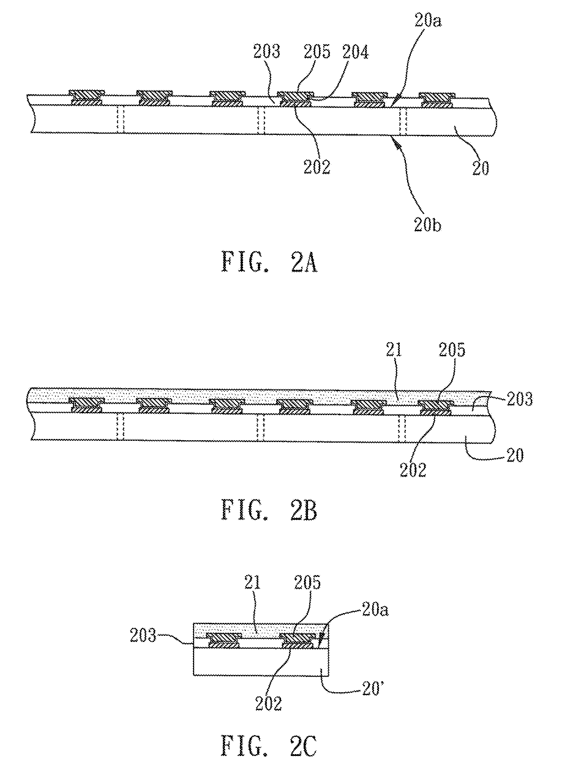
[0019]FIGS. 2A to 2G are cross-sectional views showing a preferred embodiment of a fabrication method of a circuit board structure with an embedded semiconductor chip of the present invention.

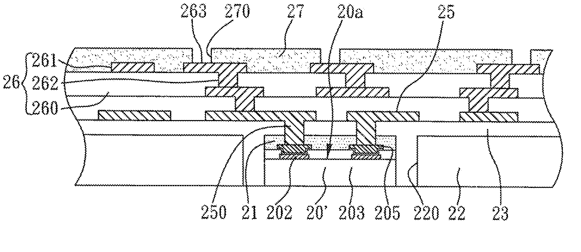
[0020]As shown in FIG. 2A, the fabrication method comprises the steps of: providing a semiconductor wafer 20 having an active surface 20a and a non-active surface 20b, wherein the active surface 20a is opposite the non-active surface 20b and disposed with a plurality of electrode pads 202; forming a passivation layer 203 on the active surface 20a of the semiconductor wafer 20; forming openings 204 in the exposed surface of the passivation layer 203 to expose the electrode pads 202 of the semiconductor wafer 20; and forming a conn...


PUM


Abstract

A circuit board structure with an embedded semiconductor chip and a fabrication method thereof are provided, including the steps of providing a semiconductor wafer having an active surface with a plurality of electrode pads, a connection metal layer formed on the electrode pads: forming a protective layer on the connection metal layer and the semiconductor wafer, performing a cutting process to form a plurality of semiconductor dies, providing a carrier board having at least on e cavity for receiving the semiconductor chip; and forming sequentially on the protective layer covering the semiconductor chip and the carrier board a dielectric layer and a circuit layer electrically connected to the connection metal layer of the semiconductor chip. The present invention is a simple, in process and low in process cost, due to the connection metal layer covered by the protective layer formed on the semiconductor chip protected from oxidation and contamination.

Description

BACKGROUND OF THE INVENTION[0001]1. Field of the Invention[0002]The present invention relates to a circuit board structure with an embedded semiconductor chip and a fabrication method thereof, and more particularly, to a circuit board structure for embedding a semiconductor chip in a circuit board and a fabrication method thereof.[0003]2. Description of the Prior Art[0004]The structure of semiconductor packages and chips is becoming smaller in line with the trend towards high integration. In view of this, a circuit board functioning as a semiconductor chip circuit board (hereinafter referred to as a circuit board or carrier) is generally densely disposed with electrical connection pads in order to allow a semiconductor chip mounted on the circuit board to be electrically connected to the circuit board, thereby allowing the semiconductor chip to operate. To reduce package size, the area occupied by integrated circuits (IC) may be reduced by using high circuit density, multi-pin packa...

Claims


Application Information

Patent Timeline
IPC IPC(8): H01L23/48H01L21/44
CPCH01L23/5389H01L24/19H01L24/82H01L2224/24227H01L2224/82039H01L2924/01029H01L2924/01079H01L2924/14H01L2924/1433H01L2924/18162H01L2924/19041H05K1/185H05K3/4644H05K2201/10674H05K2203/063H01L2924/01005H01L2924/01006H01L2924/01033H01L2924/01087H01L2924/014H01L24/24
Inventor HU, CHU-CHINCHEN, SHANG-WEI
Owner UNIMICRON TECH CORP
Why Eureka
Try Eureka