Method for forming circuit board structure of composite material

a technology of composite materials and circuit boards, applied in the direction of resistive material coating, liquid/solution decomposition chemical coating, superimposed coating process, etc., can solve the problems of unwelcome, uncontrollable chemical agents, and two adjacent wires that are much more susceptible to shorts

Inactive Publication Date: 2010-10-21
UNIMICRON TECH CORP
View PDF19 Cites 31 Cited by
  • Summary
  • Abstract
  • Description
  • Claims
  • Application Information

AI Technical Summary

Benefits of technology

[0008]The present invention therefore proposes a method for forming a circuit board structure of composite material. The method of the present invention is advantageous in selective deposition of electroless plating so that an over-plating is less likely to occur and the conductive material is less possible to extend to all directions along the corner of the opening of the r

Problems solved by technology

The conductive material 130 which extends to all directions along the corner of the opening of the recess obviously makes two adjacent wires much more susceptible to short, a

Method used


Image

  • Method for forming circuit board structure of composite material
  • Method for forming circuit board structure of composite material
  • Method for forming circuit board structure of composite material

Examples


Embodiment Construction

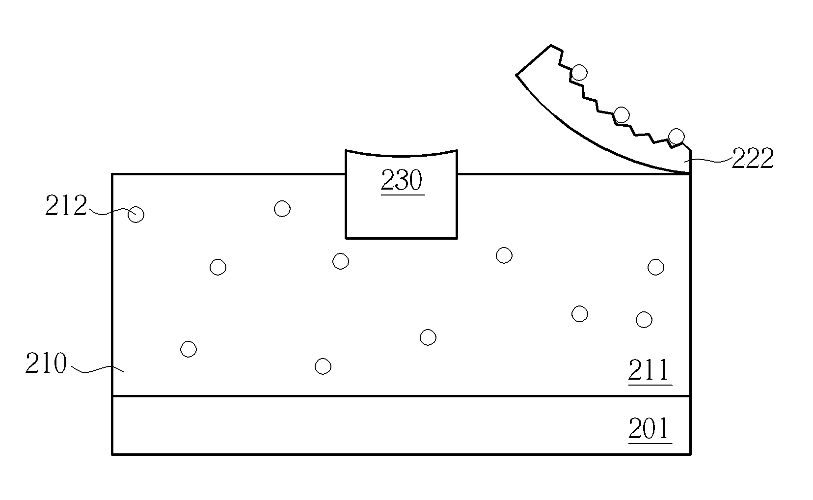
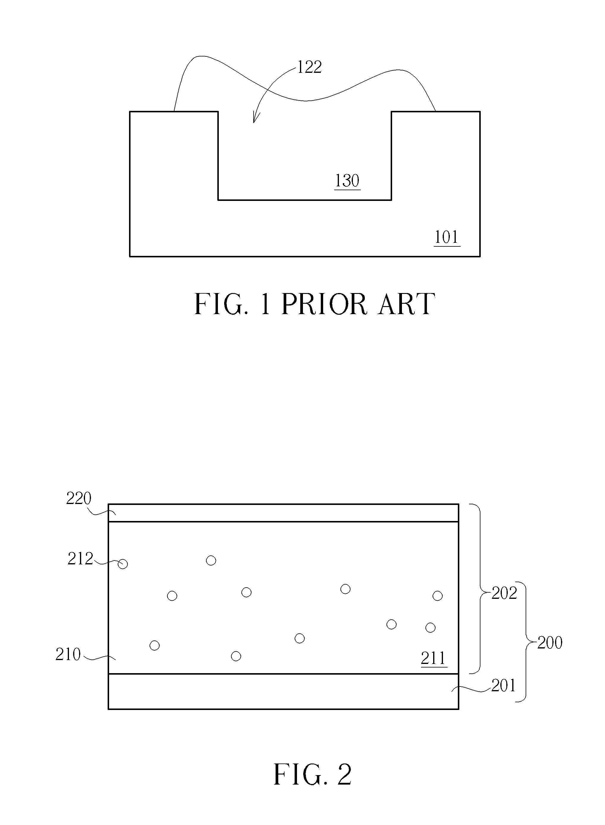
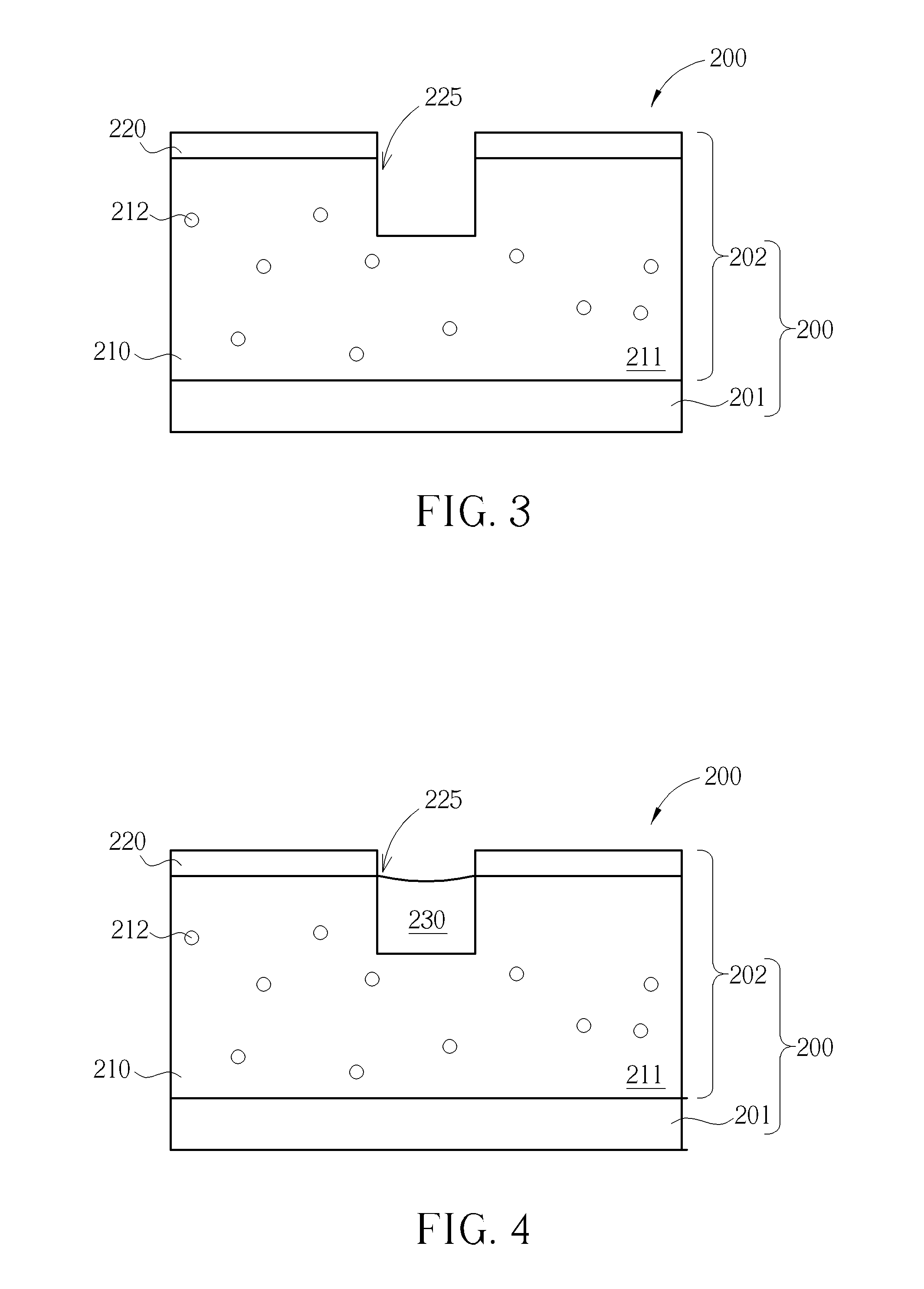
[0014]The present invention provides a method for forming a circuit board structure of composite material. The composite material in the method of the present invention is advantageous in helping selective deposition of electroless plating so that an over-plating is less likely to occur on the composite material and the conductive material is less possible to extend to all directions along the corner of the opening of the recess. In addition, the conductive material which is supposed to fill the recess on the substrate is less prone to attach to the surface of the substrate, which makes the conductive material less susceptible to depositing on the incorrect regions on the surface of the substrate and makes the wires less likely to short.

[0015]The present invention accordingly provides a method for forming a circuit board structure of composite material. FIGS. 2-7B illustrate a method for forming a circuit board structure of composite material of the present invention. As shown in FI...


PUM

PropertyMeasurementUnit
Lengthaaaaaaaaaa
Dielectric polarization enthalpyaaaaaaaaaa
Structureaaaaaaaaaa

Abstract

A method for forming a circuit board structure of composite material is disclosed. First, a composite material structure including a substrate and a composite material dielectric layer is provided. The composite material dielectric layer includes a catalyst dielectric layer contacting the substrate and at least one sacrificial layer contacting the catalyst dielectric layer. The sacrificial layer is insoluble in water. Later, the composite material dielectric layer is patterned and simultaneously catalyst particles are activated. Then, a conductive layer is formed on the activated catalyst particles. Afterwards, at least one sacrificial layer is removed.

Description

BACKGROUND OF THE INVENTION[0001]1. Field of the Invention[0002]The method of the present invention generally relates to a method for forming a circuit board structure of composite material. In particular, the method of the present invention is directed to a composite material including a catalyst particle to facilitate the formation of a circuit board structure.[0003]2. Description of the Prior Art[0004]A circuit board is an essential element in an electronic device. The embedded circuit structure draws more and more attention than ever in order to pursue a thinner product, to meet the demands of finer wires and to overcome the drawbacks of the etching procedure and reliability. Because in the embedded circuit structure the wire pattern is embedded in the substrate, the thickness of the wires seems to be omitted, thereby further reducing the thickness of the products after packaging.[0005]Currently, there are several methods available to form the circuit boards to meet the demand. ...

Claims


Application Information

Patent Timeline
IPC IPC(8): H05K3/10
CPCH05K1/036H05K1/0373H05K3/107H05K3/181H05K3/184H05K2203/308H05K2201/0236H05K2201/0257H05K2203/0264H05K2203/107H05K3/185
Inventor TSENG, TZYY-JANGYU, CHENG-POLIU, WEN-FANG
Owner UNIMICRON TECH CORP
Why Eureka
Try Eureka