Light emitting diode

a diode and light-emitting technology, applied in the field of light-emitting diodes, can solve the problems of reducing the recombination rate of electrons and holes in the active layer, reducing the luminous efficiency, and not being widely spread out on the transparent electrode layer, so as to reduce light absorption and light loss

Active Publication Date: 2009-04-30
SEOUL VIOSYS CO LTD
View PDF5 Cites 76 Cited by
  • Summary
  • Abstract
  • Description
  • Claims
  • Application Information

AI Technical Summary

Benefits of technology

[0009]This invention provides an LED having a distributed Bragg reflector (DBR) formed under a p-type

Problems solved by technology

However, in the conventional LED, current flow is concentrated just under the p-type electrode pad, and therefore, current may not be widely spread out on the transparent electrode layer.
The structure causes the recombina

Method used


Image

  • Light emitting diode
  • Light emitting diode
  • Light emitting diode

Examples


Embodiment Construction

[0018]Hereinafter, embodiments of the present invention will be described in detail with reference to the accompanying drawings. The following embodiments are provided only for illustrative purposes so that those skilled in the art can fully understand the spirit of the present invention. Therefore, the present invention is not limited to the following embodiments but may be implemented in other forms. In the drawings, the widths, lengths, thicknesses and the like of elements may be exaggerated for convenience of illustration. Like reference numerals indicate like elements throughout the specification and drawings.

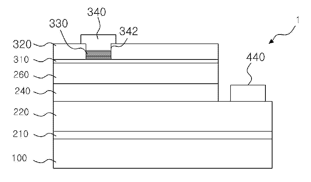
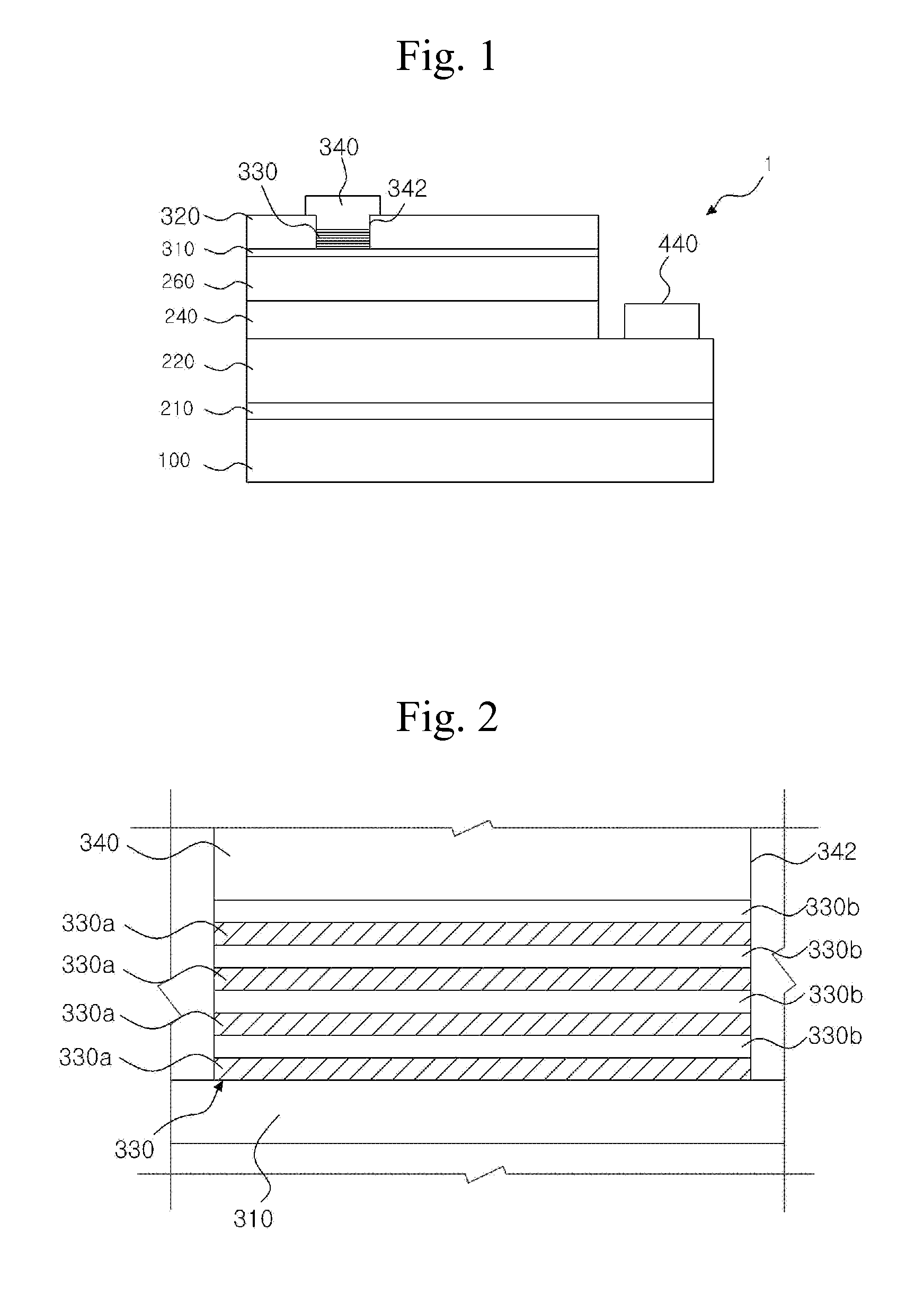
[0019]FIG. 1 is a sectional view of an LED according to an embodiment of the present invention, and FIG. 2 is a sectional view illustrating a DBR structure of the LED shown in FIG. 1.

[0020]Referring to FIG. 1, an LED 1 includes an n-type semiconductor layer 220, an active layer 240, and a p-type semiconductor layer 260, which are all arranged on a substrate 100. The active...


PUM


Abstract

A light emitting diode (LED) has an n-type semiconductor layer, an active layer, a p-type semiconductor layer, and a transparent electrode layer. The LED includes a tunnel layer interposed between the p-type semiconductor layer and the transparent electrode layer, an opening arranged in the transparent electrode layer so that the tunnel layer is exposed, a distributed Bragg reflector (DBR) arranged in the opening, and an electrode pad arranged on the transparent electrode layer to cover the DBR in the opening.

Description

CROSS REFERENCE TO RELATED APPLICATION[0001]This application claims priority from and the benefit of Korean Patent Application No. 10-2007-0108686, filed on Oct. 29, 2007, which is incorporated by reference for all purposes as if fully set forth herein.BACKGROUND OF THE INVENTION[0002]1. Field of the Invention[0003]The present invention relates to a light emitting diode (LED), particularly a GaN-based LED, and more particularly, to an LED having enhanced current spreading and light extraction efficiencies by incorporating a layer between a semiconductor layer and an electrode pad.[0004]2. Discussion of the Background[0005]An LED is a photoelectric conversion device that emits light through recombination of electrons and holes when current is applied. As an example, a GaN-based LED has an n-type semiconductor layer, an active layer, and a p-type semiconductor layer, which are sequentially arranged on a substrate. A transparent electrode layer is arranged on the p-type semiconductor l...

Claims


Application Information

Patent Timeline
IPC IPC(8): H01L33/00H01L33/42H01L33/06H01L33/10H01L33/32
CPCH01L33/105H01L33/46H01L33/465H01L33/42
Inventor KIM, HWA MOKKIM, DAE WONKAL, DAE SUNG
Owner SEOUL VIOSYS CO LTD
Why Eureka
Try Eureka