Semiconductor device
- Summary
- Abstract
- Description
- Claims
- Application Information
AI Technical Summary
Benefits of technology
Problems solved by technology
Method used
Image

Examples
first embodiment
Modified Example of First Embodiment
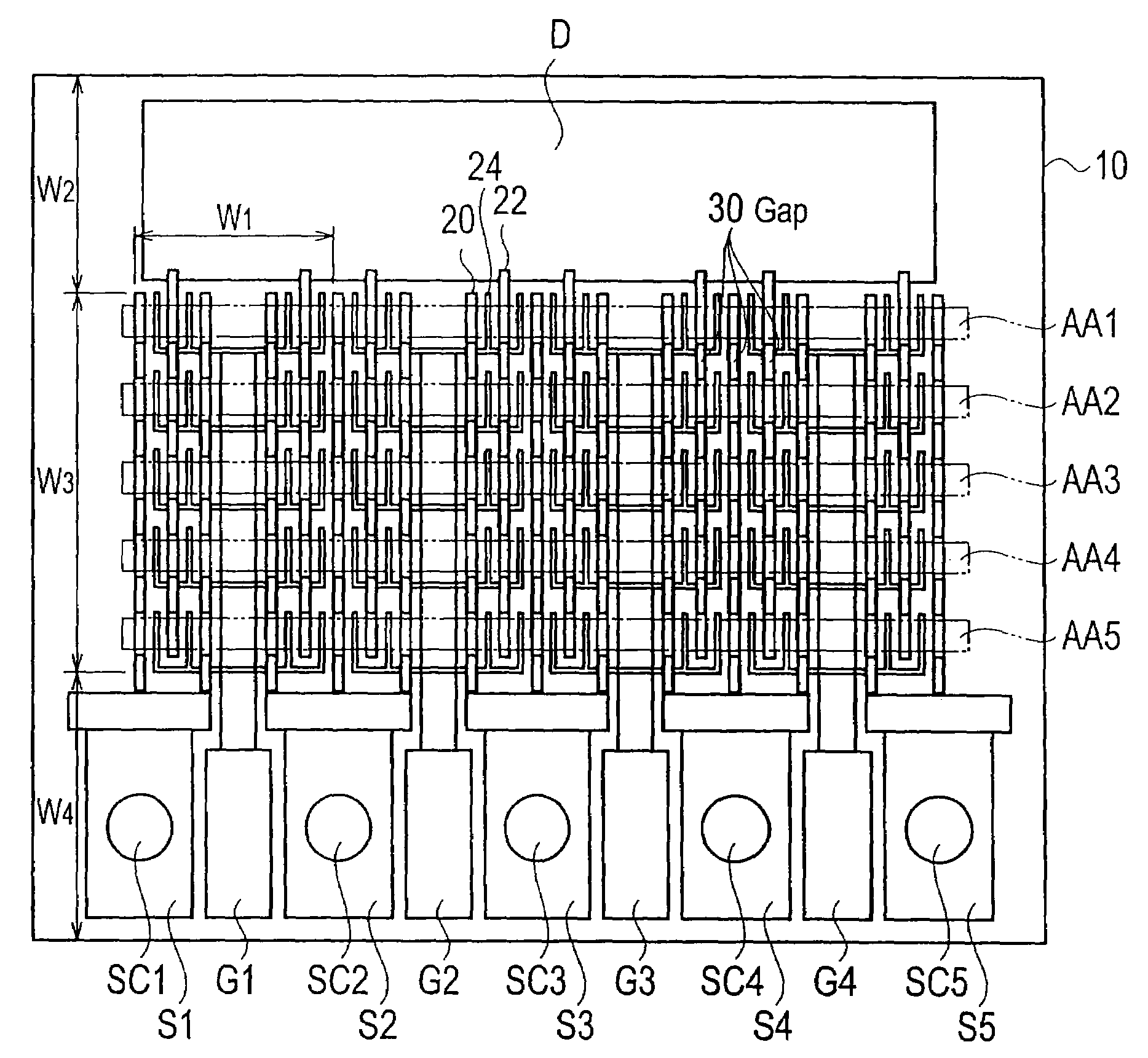
[0094]A schematic plane pattern configuration of a semiconductor device according to a modified example of the first embodiment of the present invention is expressed as shown in FIG. 3.
[0095]As shown in FIG. 3, the semiconductor device according to the modified example of the first embodiment of the present invention includes: a substrate 10; a gate electrode 24, a source electrode 20, and a drain electrode 22 which are placed on a first surface of the substrate 10 and have a plurality of fingers, respectively; gate terminal electrodes G1, G2, . . . , G4, source terminal electrodes S1, S2, . . . , S5, and the drain terminal electrode D which are placed on the first surface of the substrate 10, and governs and forms a plurality of fingers, respectively every the gate electrode 24, the source electrode 20, and drain electrode 22; active areas AA1, AA2, . . . , AA5 placed on the substrate 10 of the lower part of the gate electrode 24, the source elec...
second embodiment
Modified Example of Second Embodiment
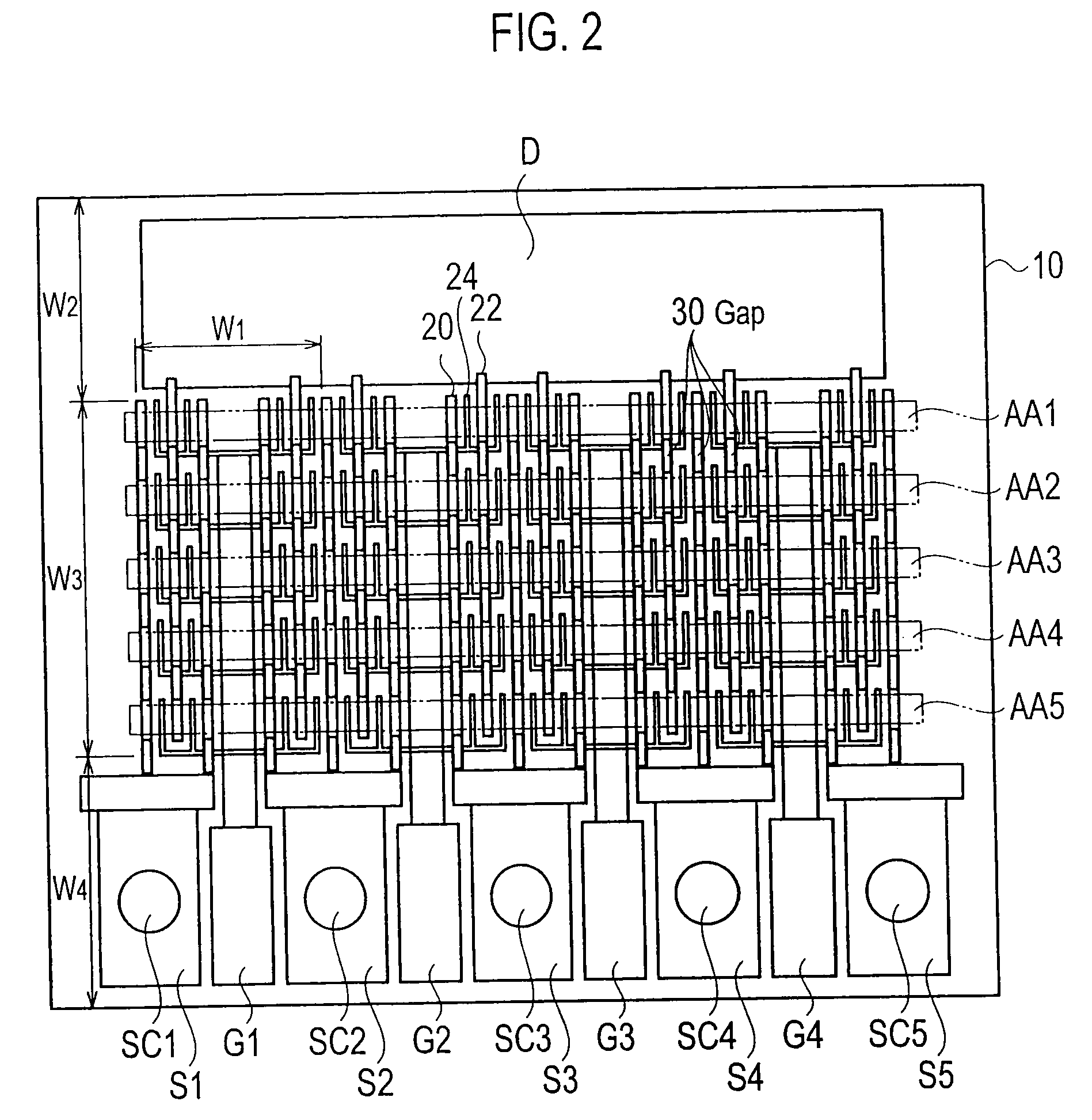
[0121]A schematic plane pattern configuration of a semiconductor device according to a modified example of the second embodiment of the present invention is expressed as shown in FIG. 7.
[0122]As shown in FIG. 7, the semiconductor device according to the modified example of the second embodiment of the present invention includes: a substrate 10; a gate electrode 24, a source electrode 20, and a drain electrode 22 which are placed on a first surface of the substrate 10 and have a plurality of fingers, respectively; gate terminal electrodes G1, G2, . . . , G6 and the source terminal electrodes S1, S2, . . . , S13, and the drain terminal electrode D which are placed on the first surface of the substrate 10, and governs and forms a plurality of fingers, respectively every the gate electrode 24, the source electrode 20, and the drain electrode 22; active areas AA1, AA2, . . . , AA7 placed on the substrate 10 of the lower part of the gate electrode 24, ...
PUM
 Abstract
Description
Claims
Application Information
 - R&D Engineer
- R&D Manager
- IP Professional
- Industry Leading Data Capabilities
- Powerful AI technology
- Patent DNA Extraction
Browse by: Latest US Patents, China's latest patents, Technical Efficacy Thesaurus, Application Domain, Technology Topic.
© 2024 PatSnap. All rights reserved.Legal|Privacy policy|Modern Slavery Act Transparency Statement|Sitemap