

Field-Through Compensation Circuit and Display Device
a compensation circuit and display device technology, applied in the field of display devices, can solve the problems of image deterioration and generation of field-through voltage, and achieve the effect of reducing field-through voltage and reducing differen
- Summary
- Abstract
- Description
- Claims
- Application Information
AI Technical Summary
Benefits of technology
Problems solved by technology
Method used
Image

Examples
first embodiment
[0032]The following will explain embodiments of the present invention with reference to the drawings.
[0033]First, an explanation will be given of a configuration of a display device 1 of a first embodiment of the present invention.
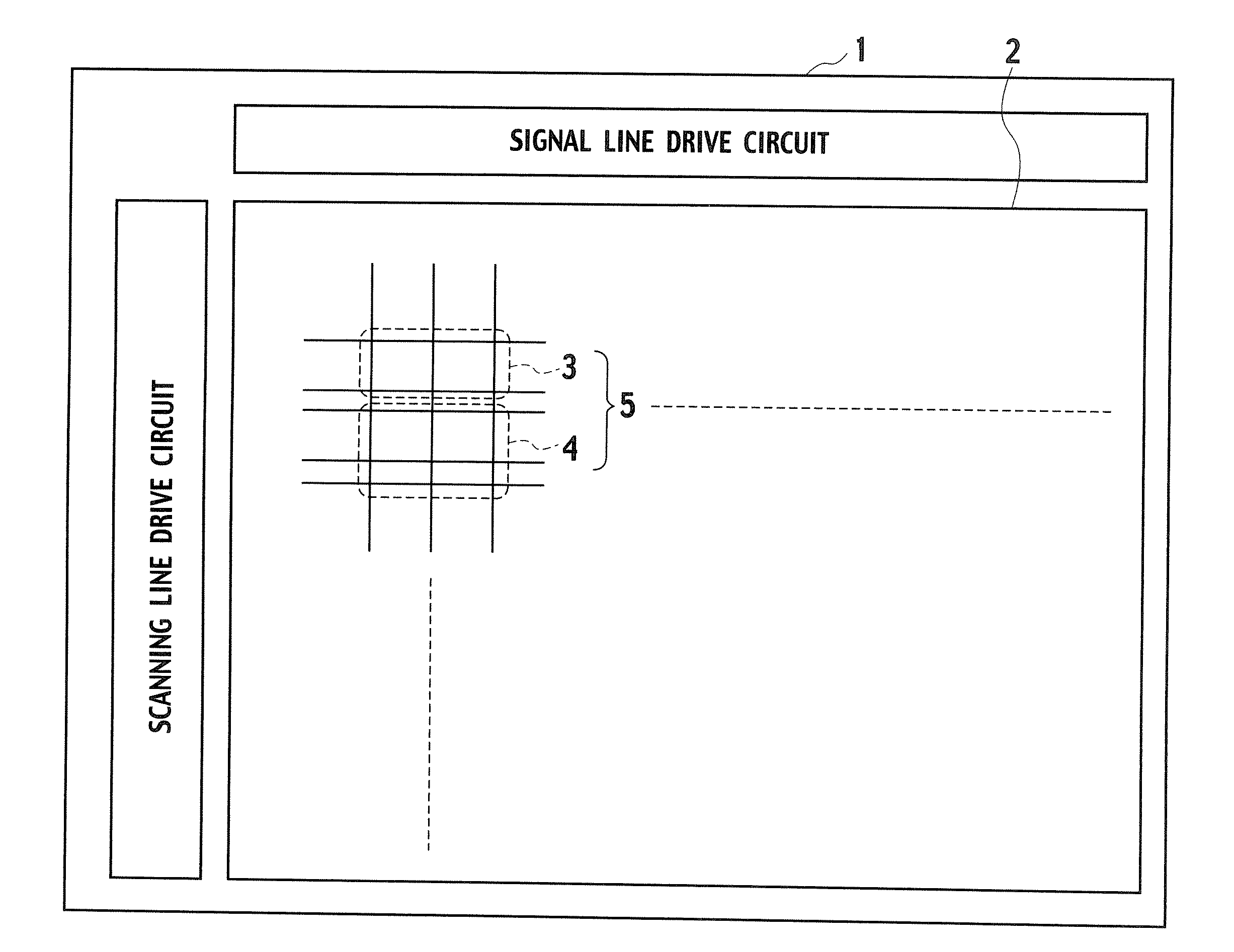
[0034]FIG. 1 is a configuration view illustrating the configuration of the display device 1 of the first embodiment of the present invention. In the display device 1 of this embodiment, multiple pixel regions 5 each having a display region 3 and an image-capturing region 4 are arranged in a display unit 2. The display region 3 has a display function of displaying an image. The image-capturing region 4 has an image-capturing function of detecting an object that has come close to the display unit 2.
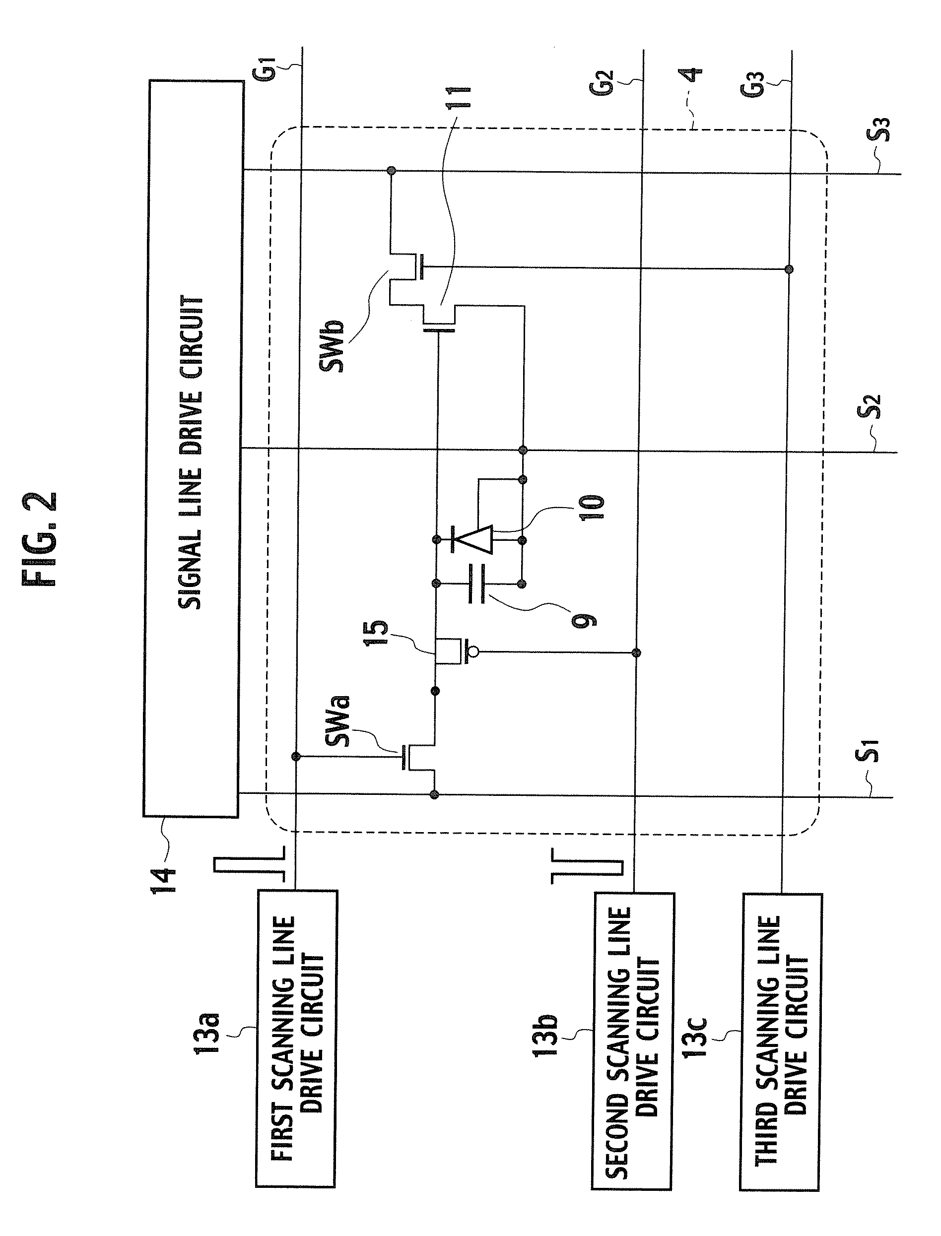
[0035]FIG. 2 is a configuration view illustrating a configuration of the image-capturing region 4 in this embodiment. The image-capturing region 4 includes as a basic configuration: first to third signal lines S1 to S3 and first to third scanning lines G1 to G3 wh...
second embodiment
[0096]FIG. 9 is a configuration view illustrating the configuration of the image-capturing region 4 in the second embodiment. The basic configuration components of the display device 1 in this embodiment are the same as those in the first embodiment and explanation of overlapped portions is omitted here.
[0097]The display device 1 of this embodiment further includes: a second input switching element SWa′; a first field-through compensation switch 15a; a second field-through compensation switch 15b; and a second scanning drive circuit 13b that controls ON / OFF of the second input switching element SWa′ and the second field-through compensation switch 15b, in addition to the basic configuration components.
[0098]In other words, the first embodiment refers to the field-through compensation for monopolar input switching elements. On the other hand, this embodiment refers to the field-through compensation for bipolar input switching elements, namely, the input switching element SWa and the ...
third embodiment
[0111]FIG. 10 is a configuration view illustrating the configuration of the image-capturing region 4 in a third embodiment. The basic configuration components of the display device 1 in this embodiment are the same as those in the first embodiment excepting the second scanning line G2, and explanation of overlapped portions is omitted here.
[0112]The first scanning line drive circuit 13a in the present display device 1 supplies the first scanning line G1a with a driving signal, having a waveform whose fall characteristic changes stepwise.
[0113]FIG. 11 is a comparison diagram illustrating comparison in an amount of the voltage stored on the respective sensor capacitors 9 at the starting end and the terminating end that are arranged on the same scanning line using the driving signal, having a waveform whose fall characteristic changes stepwise. Similar to the case in FIG. 4, a solid line indicates the waveform of the driving signal that the scanning line drive circuit 13a supplies to t...
PUM
 Abstract
Description
Claims
Application Information