Memory device, memory management method, and program
- Summary
- Abstract
- Description
- Claims
- Application Information
AI Technical Summary
Benefits of technology
Problems solved by technology
Method used
Image

Examples
Embodiment Construction
[0064]Hereinbelow, an embodiment of the present invention will be described with reference to the attached drawings.
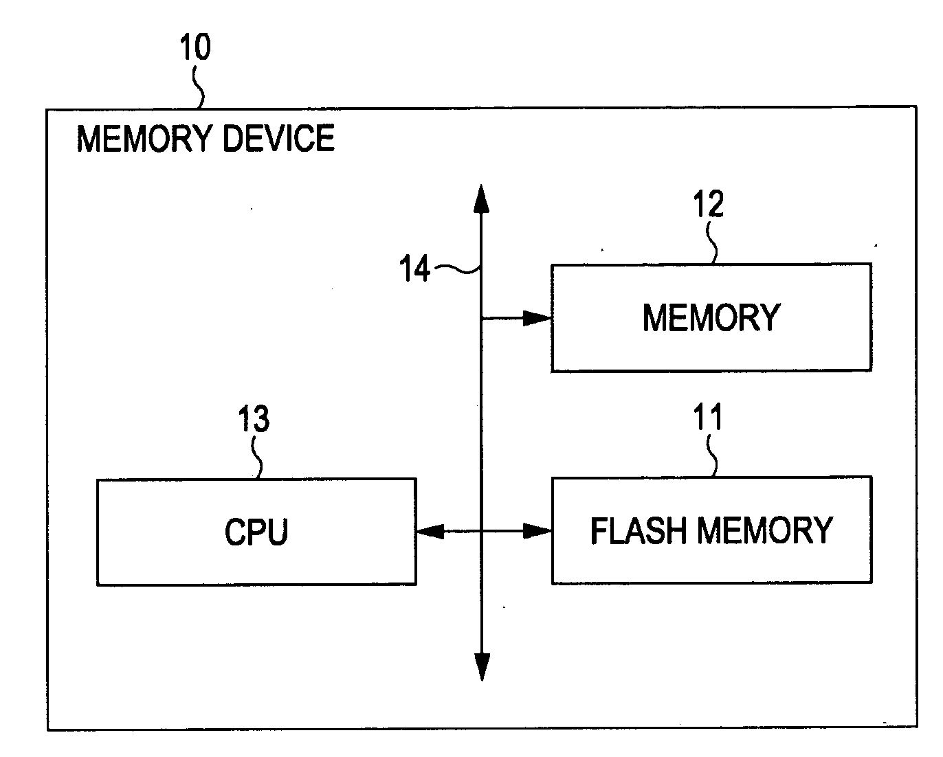
[0065]FIG. 4 is a block diagram showing an example of the basic configuration of a memory device according to an embodiment of the present invention.
[0066]A memory device 10 according to this embodiment has a NAND flash memory 11 as a non-volatile memory, a memory 12 configured by, for example, a volatile memory such as a DRAM or an SRAM, and a CPU 13 as a control section.
[0067]The NAND flash memory 11, the memory 12, and the CPU 13 are connected to each other via a bus 14.
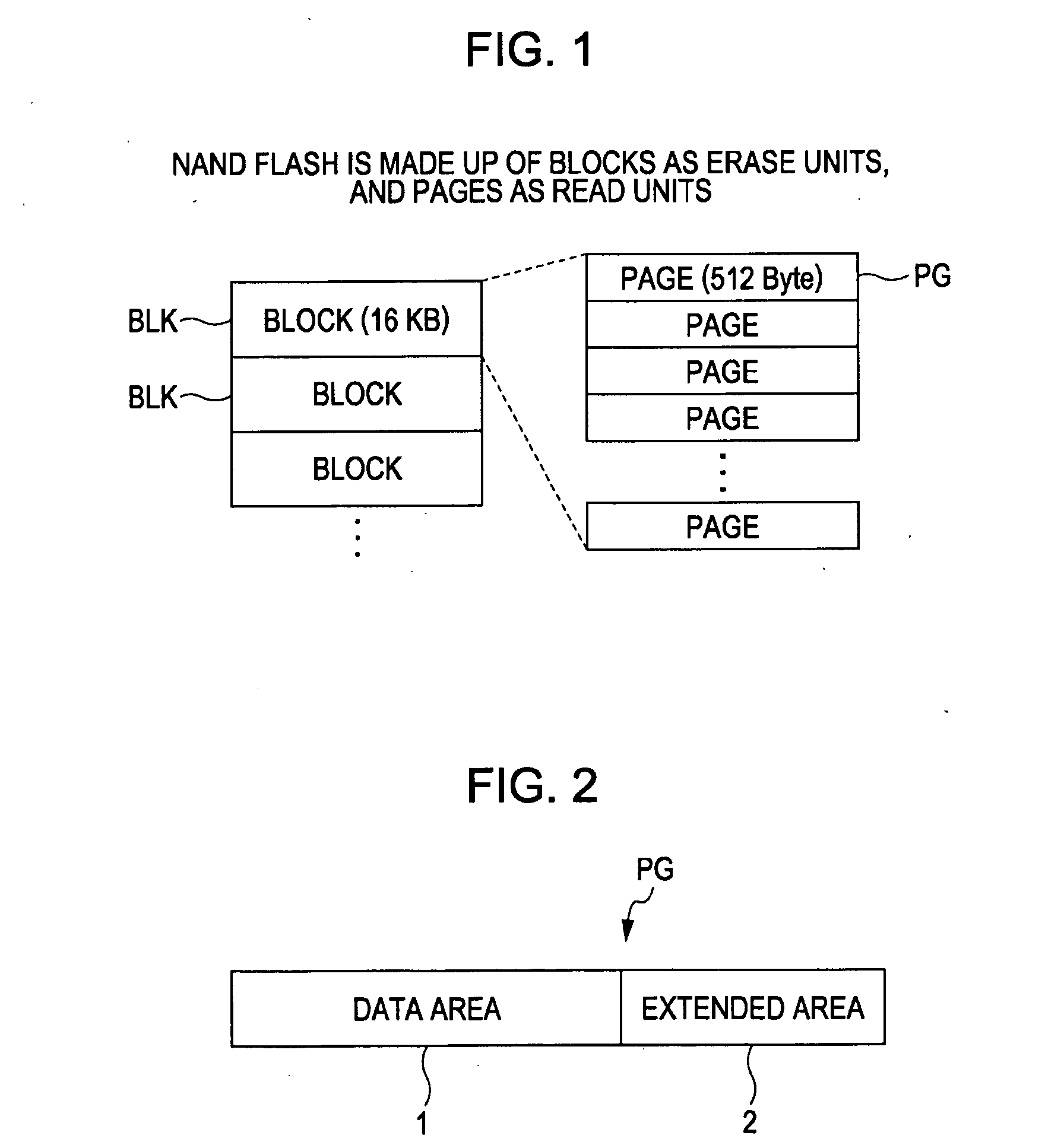
[0068]The NAND flash memory 11 has a memory cell array in which NAND strings with a plurality of memory cells connected in series are arranged in an arrayed fashion, and allows writing, reading, and erasing to be performed electrically.
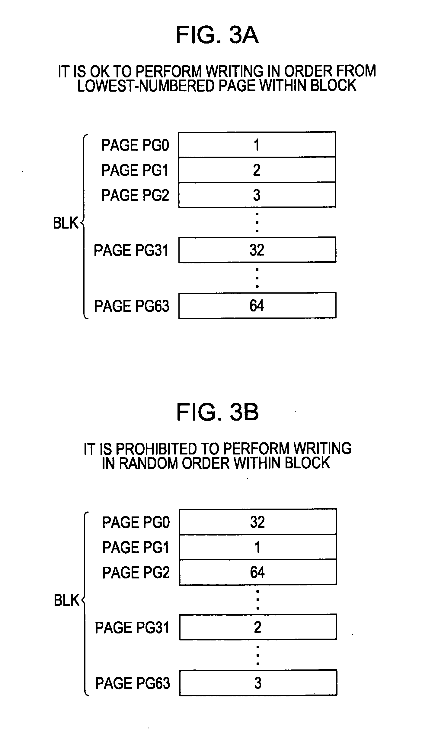
[0069]The minimum read / write unit of the NAND flash memory 11 is a page PG, and the minimum erase unit is a block BLK as a collection of a plurality of pages.
[0070]For...
PUM
 Abstract
Description
Claims
Application Information