Memory device, memory management method, and program

a memory management and memory technology, applied in the field of memory devices and memory management methods, can solve the problems of large amount of wasteful data writes and disadvantageous addition of complexity to the system configuration, and achieve the effect of improving utilization and rewriting more efficiently

Active Publication Date: 2012-06-19
SONY CORP
View PDF20 Cites 8 Cited by
  • Summary
  • Abstract
  • Description
  • Claims
  • Application Information

AI Technical Summary

Benefits of technology

[0021]The NAND flash memory described in Japanese Unexamined Patent Application Publication No. 2002-32256 allows for more efficient rewriting of data than is achieved by logical-physical translation in block units.
[0024]It is desirable to provide a memory device, a memory management method, and a program which can achieve more efficient rewriting and improved utilization, and enables a return to a normal storage state even in the event of a system down during writing or erasure at the time of a power outage or the like.
[0040]According to an embodiment of the present invention, it is possible to achieve more efficient rewriting and improved utilization, and to return to a normal storage state even in the event of a system down during writing or erasure at the time of a power outage or the like.

Problems solved by technology

Therefore, even when rewriting data of a size smaller than a block size, it is necessary to perform writing to the NAND flash memory on a block size basis, which disadvantageously results in a large amount of wasteful data writes.
However, to meet the constraint placed on the writing order of pages within a block of a NAND flash memory shown in FIGS. 3A and 3B, it is necessary to additionally provide a non-volatile memory or a data area of a NAND flash memory to store management information necessary for logical-physical translation, which disadvantageously adds complexity to the system configuration.

Method used


Image

  • Memory device, memory management method, and program
  • Memory device, memory management method, and program
  • Memory device, memory management method, and program

Examples


Embodiment Construction

[0064]Hereinbelow, an embodiment of the present invention will be described with reference to the attached drawings.

[0065]FIG. 4 is a block diagram showing an example of the basic configuration of a memory device according to an embodiment of the present invention.

[0066]A memory device 10 according to this embodiment has a NAND flash memory 11 as a non-volatile memory, a memory 12 configured by, for example, a volatile memory such as a DRAM or an SRAM, and a CPU 13 as a control section.

[0067]The NAND flash memory 11, the memory 12, and the CPU 13 are connected to each other via a bus 14.

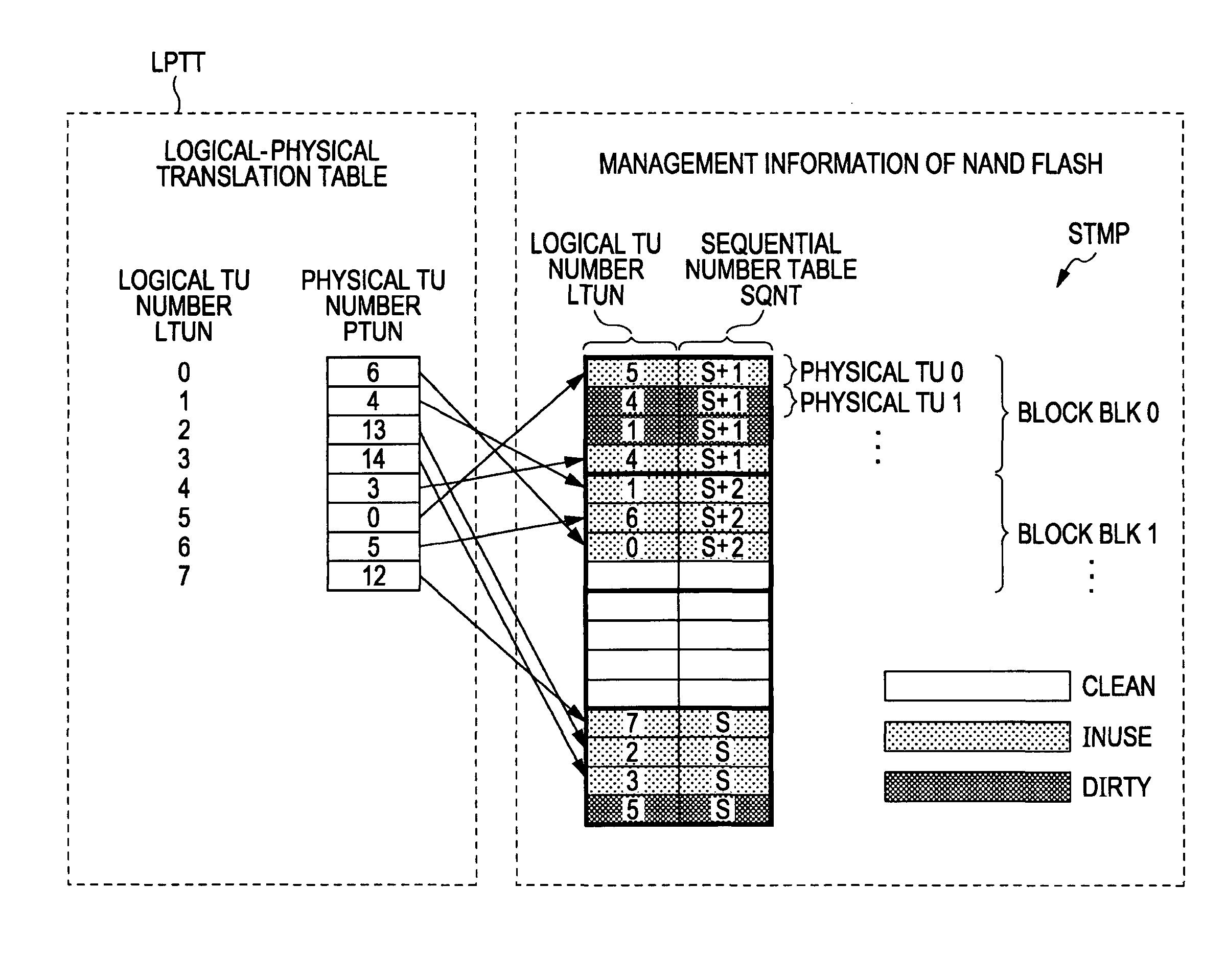
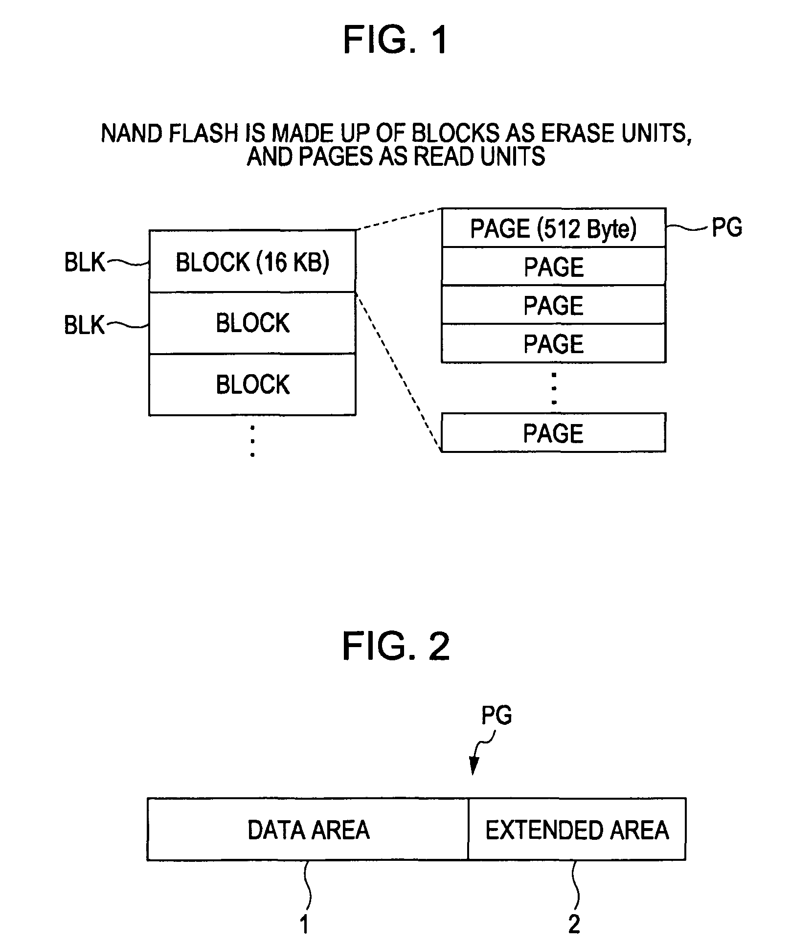
[0068]The NAND flash memory 11 has a memory cell array in which NAND strings with a plurality of memory cells connected in series are arranged in an arrayed fashion, and allows writing, reading, and erasing to be performed electrically.

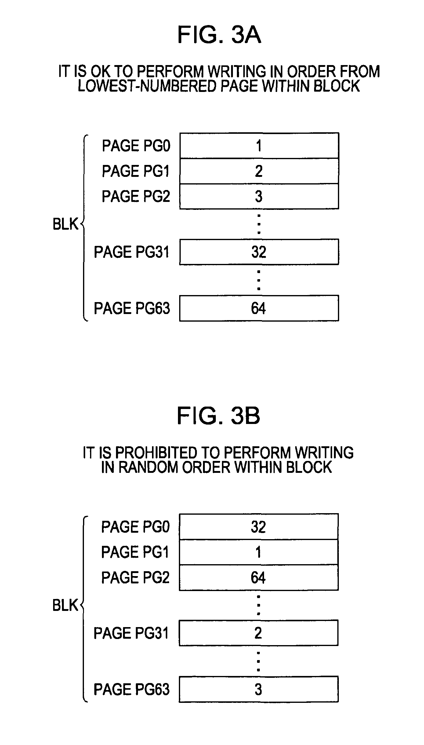
[0069]The minimum read / write unit of the NAND flash memory 11 is a page PG, and the minimum erase unit is a block BLK as a collection of a plurality of pages.

[0070]For...


PUM


Abstract

A memory device includes a non-volatile memory which allows data to be written, read, and erased electrically and in which writing and reading are done in units of a page and erasing is done in units of a block including a plurality of pages, and a control section that manages access to the non-volatile memory. The control section performs management of access to the non-volatile memory by performing logical address-physical address translation (logical-physical translation) in translation units (TUs) each being an integer fraction of a size of the block and an integer multiple of a page size.

Description

CROSS REFERENCES TO RELATED APPLICATIONS[0001]The present invention contains subject matter related to Japanese Patent Application JP 2007-288726 filed in the Japanese Patent Office on Nov. 6, 2007, the entire contents of which are incorporated herein by reference.BACKGROUND OF THE INVENTION[0002]1. Field of the Invention[0003]The present invention relates to a memory device having a non-volatile memory, a memory management method, and a program which can be applied to, for example, a NAND flash memory.[0004]2. Description of the Related Art[0005]A NAND flash memory allows data to be operated electrically, by “writing”, “reading” and “erasing”.[0006]For example, since rewriting of bits by “writing” is performed in only one direction from “1” to “0”, to write data anew, it is necessary to perform “writing” after setting all bits to “1” once by “erasing”.[0007]As shown in FIG. 1, in a NAND flash memory, the minimum unit of writing / reading is a page PG, and the minimum unit of “erasing...

Claims


Application Information

Patent Timeline
Patent Type & Authority Patents(United States)
IPC IPC(8): G06F12/00G11C16/02
CPCG06F12/0246G06F2212/7209
Inventor SAEKI, SHUSUKEIWASAKI, SATORUICHIMORI, SEIYANAGAHAMA, HIROKISATO, KAZUMI
Owner SONY CORP
Why Eureka
Try Eureka