Nonvolatile semiconductor memory device and method of driving the same
- Summary
- Abstract
- Description
- Claims
- Application Information
AI Technical Summary
Benefits of technology
Problems solved by technology
Method used
Image

Examples
first embodiment
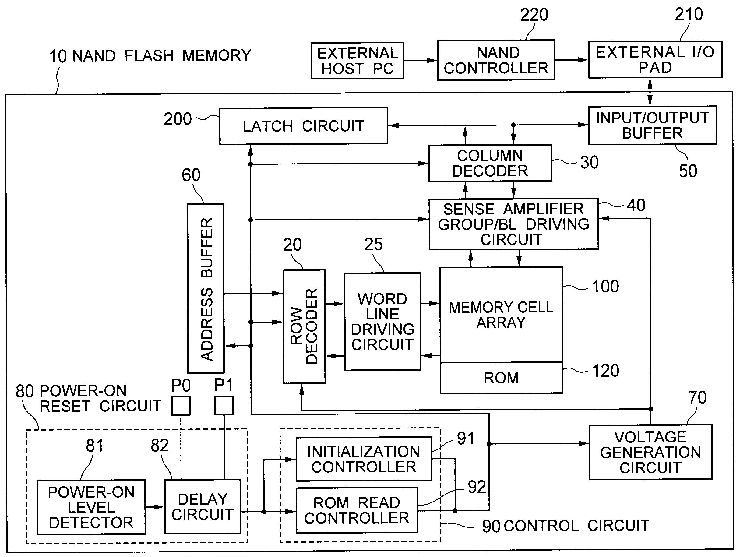
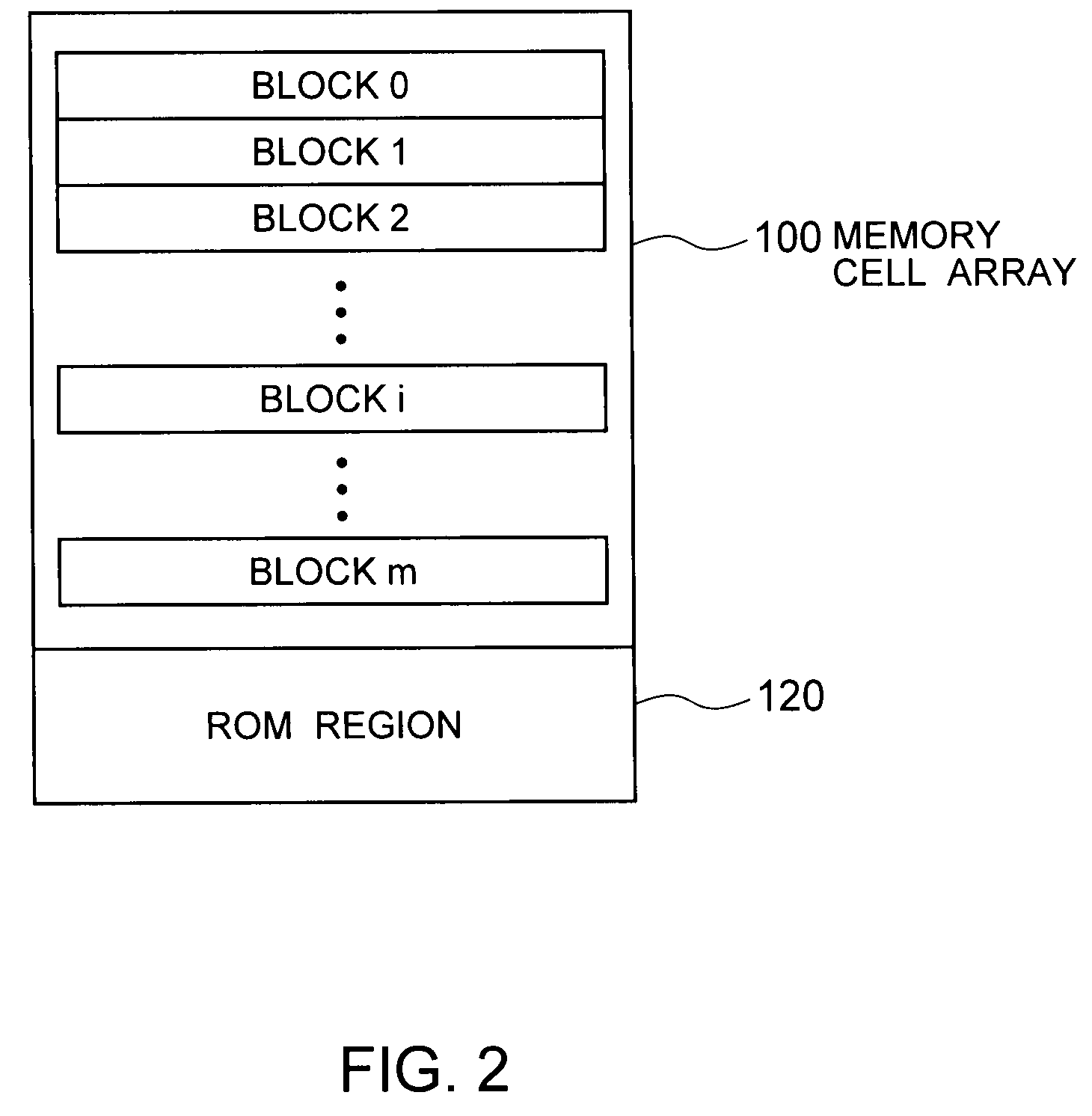
[0034]FIG. 1 is a block diagram showing an example of a configuration of a NAND flash memory 10 (hereinafter, simply “memory 10”) according to a first embodiment of the present invention. The memory 10 includes a memory cell array 100, a row decoder 20, a word line driving circuit 25, a column decoder 30, a sense amplifier group / bit line driving circuit 40 (hereinafter, simply, “sense amplifier” or “bit line driving circuit”), an input / output buffer 50, an address buffer 60, a voltage generation circuit 70, a power ON reset circuit 80, a control circuit 90, a latch circuit 200, an external I / O pad 210, and a NAND controller 220. While the memory 10 also includes a state machine, a command interface or the like, they are not shown in FIG. 1.
[0035]The NAND controller 220 outputs data and a control signal (command). The data and the control signal are input to the input / output buffer 50 via the external I / O pad. The input / output buffer 50 transmits the data and the control signal to th...
second embodiment
[0079]FIG. 7 is a flowchart showing the data write operation to the first cell block and the verifying operation of the written data according to a second embodiment of the present invention (a modified example of the first write sequence). The second embodiment differs in first write sequence from that of the first embodiment.
[0080]First, a word line WLn at a certain address is selected (S7). The data to be written to the memory cells MCs connected to the selected word lines WLn and WLn+1 are loaded from the outside of the memory 10 (S12). Subsequently, the data “1” are written to the first cell block (S22 and S24). At this time, the word line driving circuits 25 and the bit line driving circuits continuously select the two adjacent word lines WLn and WLn+1. The bit line driving circuit firstly writes the data to the memory cells MCs connected to the word line WLn, and thereafter, writes the data to the memory cells MCs connected to the word line WLn+1. As a result, the bit line dr...
third embodiment
[0085]FIG. 8A is a conceptual diagram showing a method for writing the multivalued data to the first cell block according to a third embodiment of the present invention. FIG. 8B shows a comparative example of the method for writing data. After the verifying operation, the memory 10 uses an LM (Lower Middle) method, for example, to write four-valued data (2-bit data) to the first cell block.
[0086]Hereinafter, the LM method is described. For example, each the memory cell MC stores therein one of the four-valued data (11, 10, 01, and 00). A lower bit of the four-valued data is stored as Lower Page data and an upper bit thereof is stored as Upper Page data in each memory cell MC. In FIG. 8A and FIG. 8B, a write order of the Lower Page data is indicated by a lower semicircle, and a write order of the Upper Page data is indicated by an upper semicircle.
[0087]In the LM method, the writing of the four-valued data is executed by two operations of a Lower Page write operation and an Upper Pag...
PUM
 Abstract
Description
Claims
Application Information
 - R&D Engineer
- R&D Manager
- IP Professional
- Industry Leading Data Capabilities
- Powerful AI technology
- Patent DNA Extraction
Browse by: Latest US Patents, China's latest patents, Technical Efficacy Thesaurus, Application Domain, Technology Topic.
© 2024 PatSnap. All rights reserved.Legal|Privacy policy|Modern Slavery Act Transparency Statement|Sitemap