Mos capacitor structure and linearization method for reduced variation of the capacitance

a capacitor and linearization technology, applied in the field ofmos capacitors, can solve the problems of inability to provide adequate stable or linear response of the capacitor for certain applications, and high variation of the capacitance value may not be desirabl

Inactive Publication Date: 2009-05-21
AVAGO TECH WIRELESS IP SINGAPORE PTE
View PDF6 Cites 39 Cited by
  • Summary
  • Abstract
  • Description
  • Claims
  • Application Information

AI Technical Summary

Problems solved by technology

Because of this variation, the capacitor may not have an adequate stable or linearized response for certain applications.
For circuits such as oscillators, phase-

Method used


Image

  • Mos capacitor structure and linearization method for reduced variation of the capacitance
  • Mos capacitor structure and linearization method for reduced variation of the capacitance
  • Mos capacitor structure and linearization method for reduced variation of the capacitance

Examples


Embodiment Construction

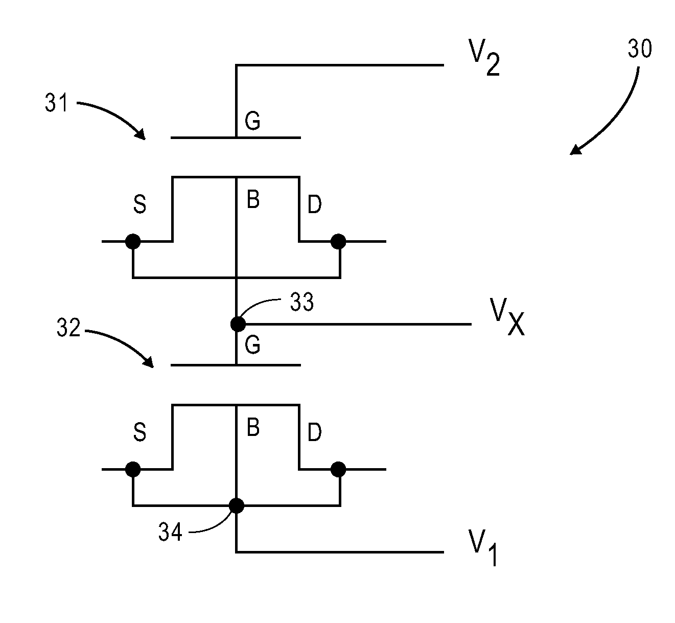
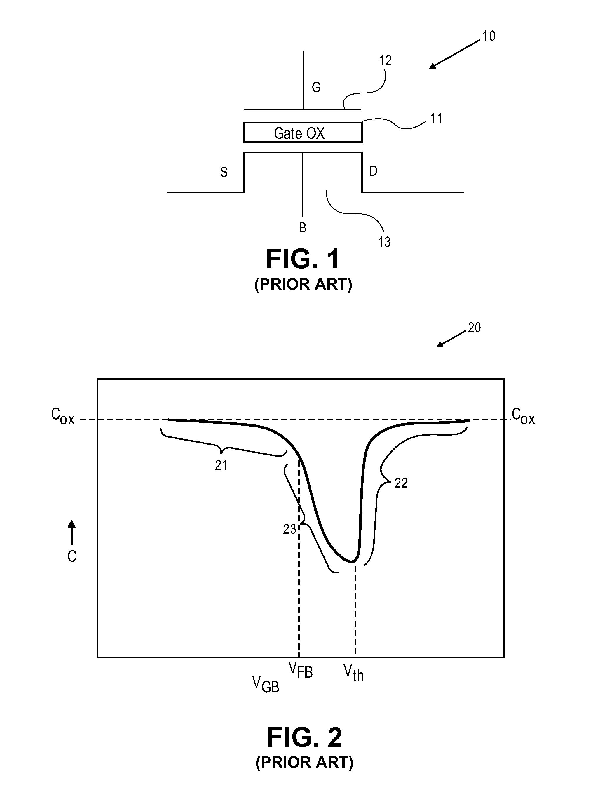
[0017]The embodiments of the present invention may be practiced in a variety of settings that implement a Metal-Oxide-Semiconductor (MOS) capacitor structure. The specific embodiments described below pertain to an n-type MOS (NMOS) device, but is equally applicable to p-type (PMOS) devices as well. Generally, MOS capacitors are manufactured using a silicon substrate, however, the capacitor structure may be readily adapted to other technologies that use other substrate materials.

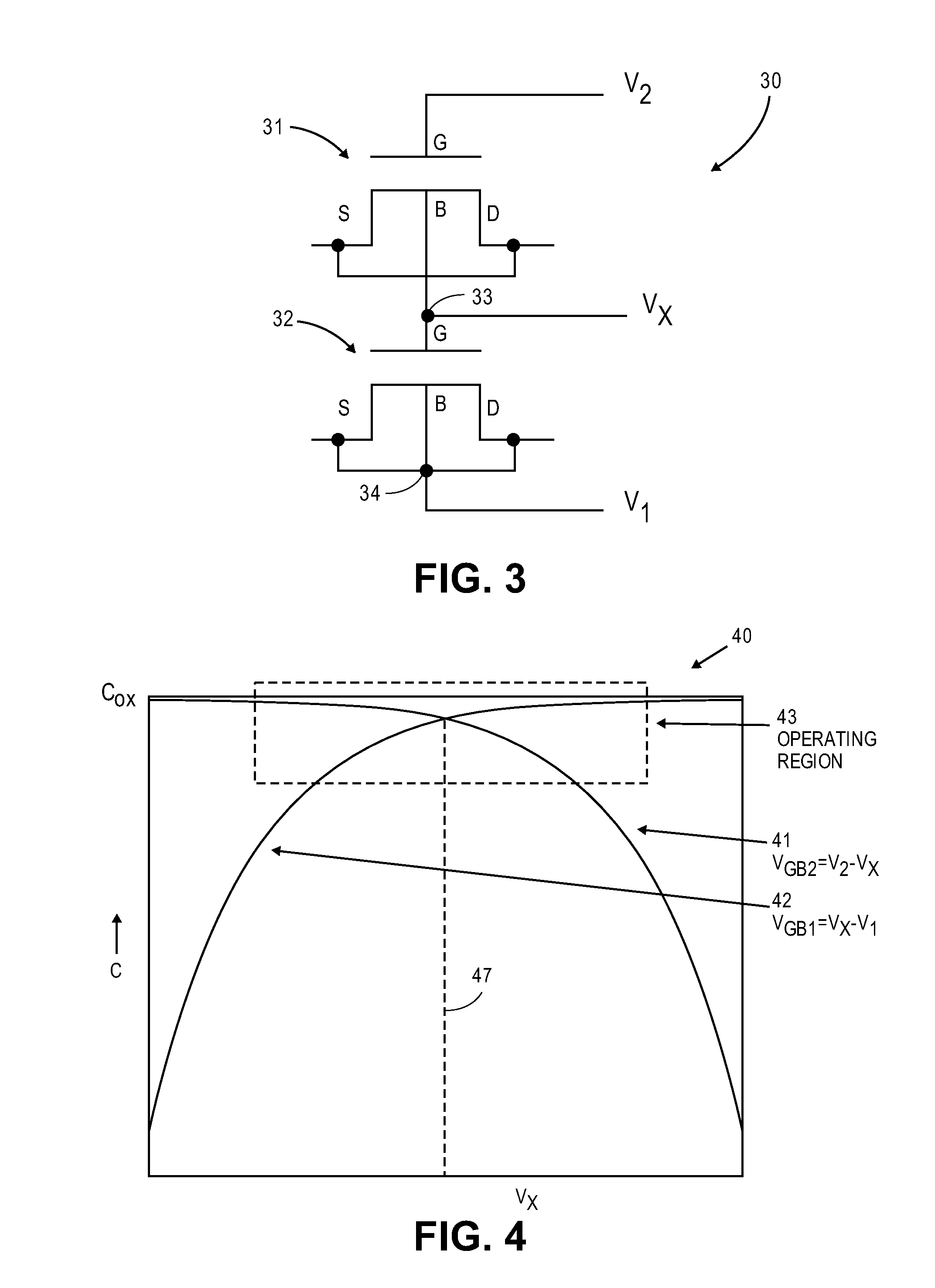
[0018]FIG. 3 illustrates one embodiment of the invention in which two MOS capacitors are coupled together to combine their characteristics to provide a more linearized and reduced variation response over the single prior art capacitor of FIG. 1. In FIG. 3, a MOS capacitor structure 30 is shown comprised of MOS capacitor 31 and MOS capacitor 32. In this example, both capacitors 31, 32 are n-type (NMOS) devices. However, as noted below, the capacitor structure may be constructed using p-type (PMOS) capacitors a...


PUM


Abstract

A highly linearized capacitor structure is formed by a first capacitor, that is coupled between a first terminal and a common node, combine with a second capacitor, that is coupled between a second terminal and the common node. When a bias voltage is applied, the capacitance values of the first and second capacitors combine and a capacitance variation of the first capacitor is compensated by a capacitance variation of the second capacitor to reduce and linearize overall capacitance variation in the combined capacitor structure.

Description

BACKGROUND OF THE INVENTION[0001]1. Technical Field of the Invention[0002]The present invention relates generally to MOS capacitors and, more particularly, to MOS capacitors for use in wireless devices.[0003]2. Description of Related Art[0004]Metal-Oxide-Semiconductor (MOS) capacitors are capacitor structures implemented using MOS technology. A typical structure of a MOS capacitor is shown in FIG. 1. Generally, a gate oxide layer 11 resides between a gate (G) 12 and a substrate 13, in which the gate and the substrate (also referred to as bulk material) function as the two plates of a capacitor with the gate oxide material functioning as the dielectric between the two plates. The substrate may be formed from a variety of materials, but for MOS technology, the substrate is typically silicon. Substrate 13 of FIG. 1 is designated as “B” for Bulk material. In forming MOS capacitors, the structure is designed similar to a field-effect-transistor (FET) with source (S) and drain (D) regions...

Claims


Application Information

Patent Timeline
IPC IPC(8): H01G4/38
CPCH01G4/38H01G4/255
Inventor HARALABIDIS, NIKOLAOS C.KOKOLAKIS, IOANNIS G.
Owner AVAGO TECH WIRELESS IP SINGAPORE PTE
Why Eureka
Try Eureka