

Flexible printed circuit board and manufacturing method thereof
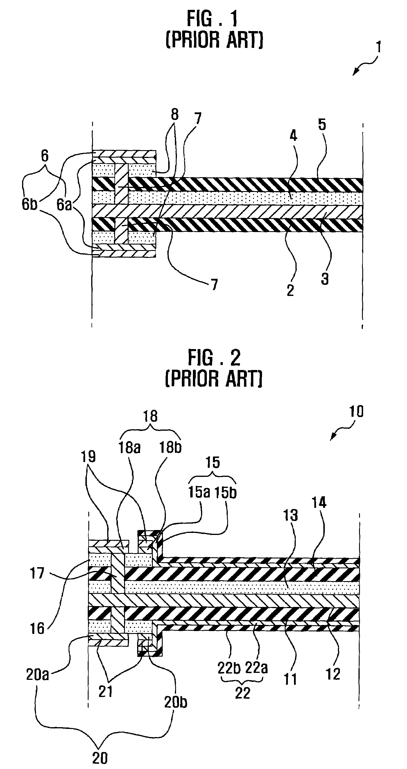
a printed circuit board and flexible technology, applied in the direction of circuit electrostatic discharge protection, overvoltage circuit protection, cross-talk/noise/interference reduction, etc., can solve the problems that the conventional fpcp such as shown in fig. 2 still suffers from the degradation of signal transmission characteristics, and achieves superior signal transmission characteristics and reduces the durability and reliability of the fpcb
- Summary
- Abstract
- Description
- Claims
- Application Information
AI Technical Summary
Benefits of technology
Problems solved by technology
Method used
Image

Examples
exemplary embodiment 3
of FPCB
[0056]FIG. 6 is a cross-sectional view illustrating an FPCB 300 according to a third exemplary embodiment of the present invention. The FPCB 300 according to the third exemplary embodiment is different from the first and second embodiments in that a shielding layer 360 is formed on only any one of the surfaces of the single layer FPCB 310 as a basic structure.
[0057]As shown in FIG. 6, the FPCB 300 according to a third exemplary embodiment of the present invention is the same as the first and second exemplary embodiments in that it has a single layer FPCB 310 as a basic structure. The single layer FPCB 310 comprises a cover insulating layer 315. A first adhesive layer 341 is formed at both ends of the upper surface of the cover insulating layer 315. A shielding insulating layer 321 is bonded to both ends of the cover insulating layer 315 by the first adhesive layer 341. A shielding layer 360 is bonded to a surface of the shielding insulating layer 321 which is opposite to the ...
exemplary embodiment 1
of FPCB Manufacturing Method
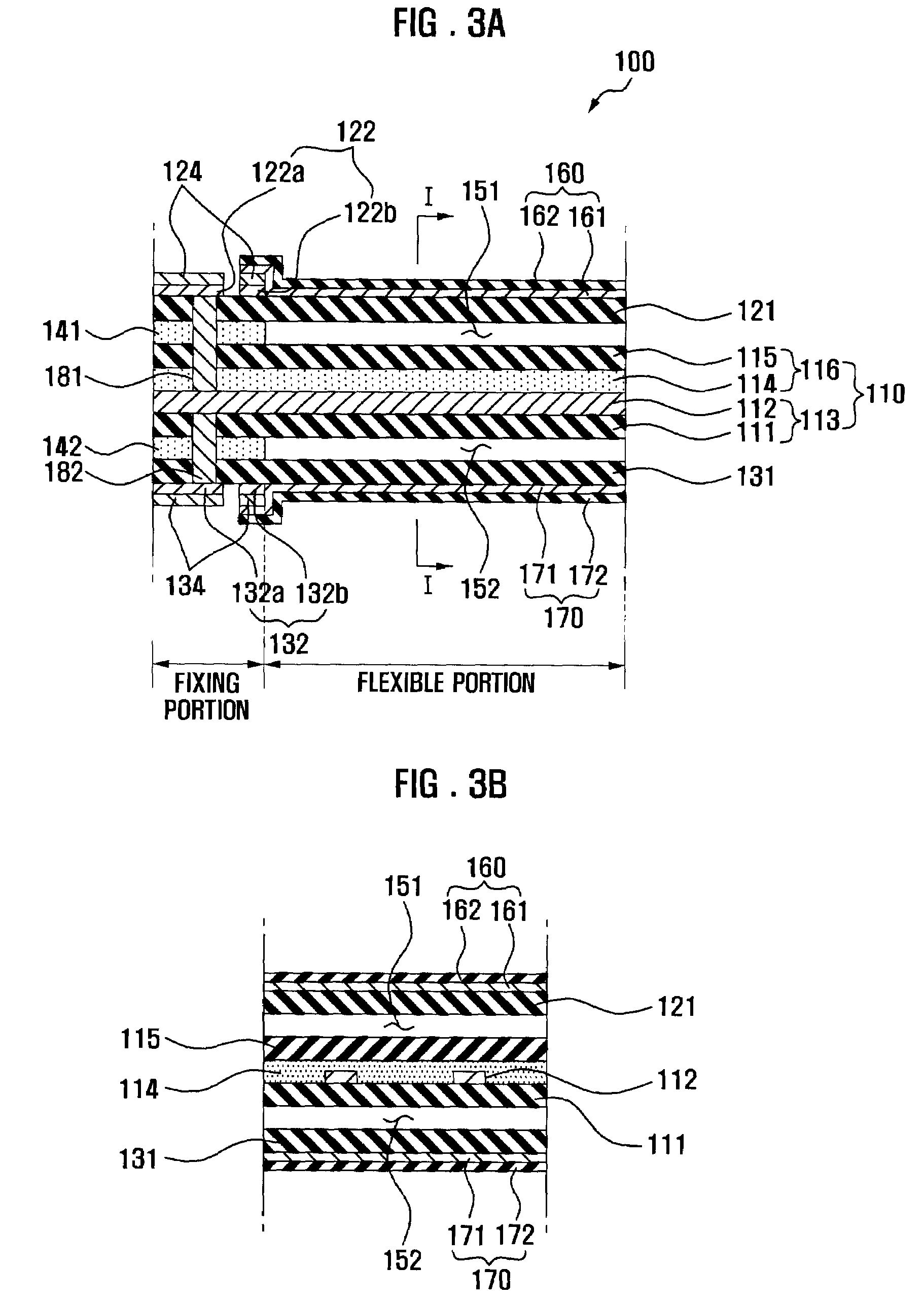
[0062]FIG. 7A to FIG. 7D are cross-sectional views that describe an FPCB manufacturing method according to a first exemplary embodiment of the present invention.
[0063]First, as shown in FIG. 7A and FIG. 7B, a first single layer FPCB 110 is prepared that is configured to include a base layer 113 and a cover layer 116 stacked on the base layer 113, where the base layer 113 comprises a base insulating layer 111 and a signal layer 112 formed thereon, and the cover layer 116 comprises an adhesive layer 114 and a cover insulating layer 115 formed thereon. A first adhesive layer 141 is bonded on the upper surface of the cover insulating layer 115 at both ends of the first single layer FPCB 110. A second single layer FPCB 120 is bonded on the first adhesive layer 141. Unlike the first single layer FPCB 110, the second single layer FPCB 120 has a base layer 123 that comprises an insulating layer 121 and a signal layer 122 formed thereon, without forming a cover la...
exemplary embodiment 2
of FPCB Manufacturing Method
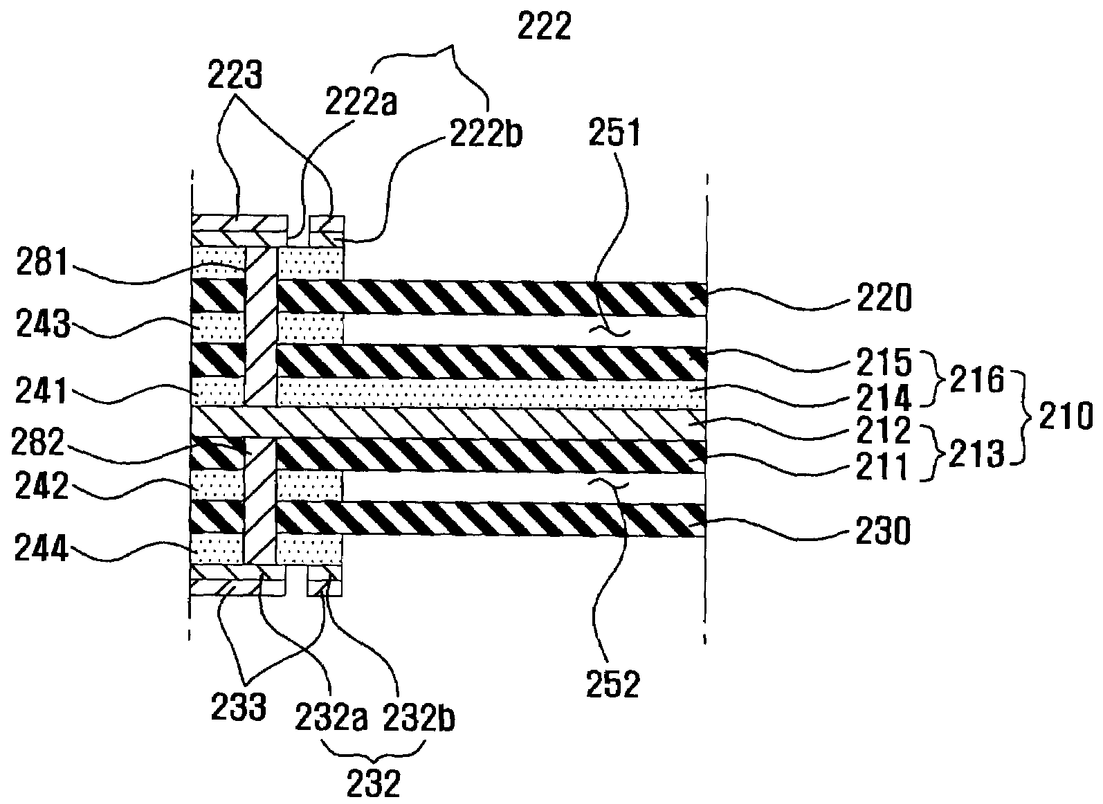
[0068]FIG. 8A to FIG. 8C are cross-sectional views that describe an FPCB manufacturing method according to a second exemplary embodiment of the present invention.
[0069]First, as shown in FIG. 8A, a single layer FPCB 210 is prepared that is stacked in order with an insulating layer 211, a signal layer 212, an adhesive layer 214 and a cover insulating layer 215. A first adhesive layer 241 is bonded on the upper surface of the cover insulating layer 215 at both ends of the single layer FPCB 210. After that, a first insulating layer 220 made of a dielectric material is bonded to the first adhesive layer 241, forming a first space 251 between the first insulating layer 220 and the cover insulating layer 215. Unlike the insulating layer 121 of the second single layer FPCB 120 that is formed by the method according to the first exemplary embodiment, the first insulating layer 220 comprises a single insulating layer preferably made of a dielectric material. There...
PUM
| Property | Measurement | Unit |
|---|---|---|
| thick | aaaaa | aaaaa |
| thick | aaaaa | aaaaa |
| thick | aaaaa | aaaaa |
Abstract
Description
Claims
Application Information