Plasma display panel and method for manufacturing the same

a technology of plasma and display panel, which is applied in the manufacture of electrode systems, electric discharge tubes/lamps, electrodes, etc., can solve the problems of a small chance of discharge completion, a time lag, and a generation evidently occurring, so as to reduce the surface free energy and reduce the chance of discharge completion. , the effect of large secondary electron emission coefficient and smooth emission

Active Publication Date: 2009-06-04
PANASONIC CORP
View PDF7 Cites 38 Cited by
  • Summary
  • Abstract
  • Description
  • Claims
  • Application Information

AI Technical Summary

Benefits of technology

[0025]According to the present invention with the above structure, the MgO powder is characterized by the Mgo particles having the (100) crystal face and the (111) crystal face (herein after, referred to as “two specific crystal faces”).
[0026]The (100) crystal face, with its lowest surface free energy, barely absorbs impurity gas (water, hydrocarbon, carbon dioxide, etc.) in a wide temperature range from a low temperature to a temperature equal to or higher than a normal temperature. Thus, the (100) crystal face stably emits secondary electrons at a low temperature at which impurity gas is easily absorbed. Furthermore, the (111) crystal face has a large secondary electron emission coefficient, and therefore smoothly emits secondary electrons at a temperature equal to or higher than a normal temperature. Thus, disposing the MgO particles with the two specific crystal faces on the dielectric layer ensures a synergistic effect between the properties of each crystal face, enabling the two specific crystal faces efficiently and stably to emit secondary electrons in the wide temperature range. Consequently, the PDP in accordance with the embodiments of the present invention is able to suppress the “discharge delay,”“dependence of discharge delay on temperatures” and in the wide temperature range, and therefore can be expected to display high-definition images.
[0027]Note that the MgO powder in accordance with the present invention may include MgO particles each having the (100) crystal face, the (110) crystal face and the (111) crystal face (herein after, referred to as “three specific crystal faces”) besides the MgO particles having the two specific crystal faces. The MgO particles having the three specific crystal faces are expected to produce similar effects as the MgO particles having the two specific crystal faces. In addition to the effects, the MgO particles having the three specific crystal faces are expected to improve dependence of discharge delay on space charges.

Problems solved by technology

The first problem is that, when a pulse is applied to the display electrodes, a “discharge delay” which is a time lag between pulse application and discharge generation evidently occurs.
However, when the PDP is driven at the high speed by applying the narrowed width of data pulse, there is a smaller chance that the discharge is completed in duration of the narrowed pulse.
Therefore, there is a risk that some of the discharge cells are not addressed properly thereby failing to light.
The second problem is that the temperature dependency on discharge delay increases with increase in Xe gas concentration in the discharge gas.
More specifically, a high content of the Xe gas causes the discharge delay to be more dependent on temperatures, especially at a low temperature.
Thus, the occurrence of the discharge delay becomes more problematic.
This problem is actually crucial in the initial stage of driving the PDP.
The third problem is that the higher the concentration of Xe gas in the discharge gas is, the more dependent on the number of sustain pulses the discharge delay is (dependence of discharge delay on space charges).

Method used


Image

  • Plasma display panel and method for manufacturing the same
  • Plasma display panel and method for manufacturing the same
  • Plasma display panel and method for manufacturing the same

Examples


embodiment 1

Structure of PDP

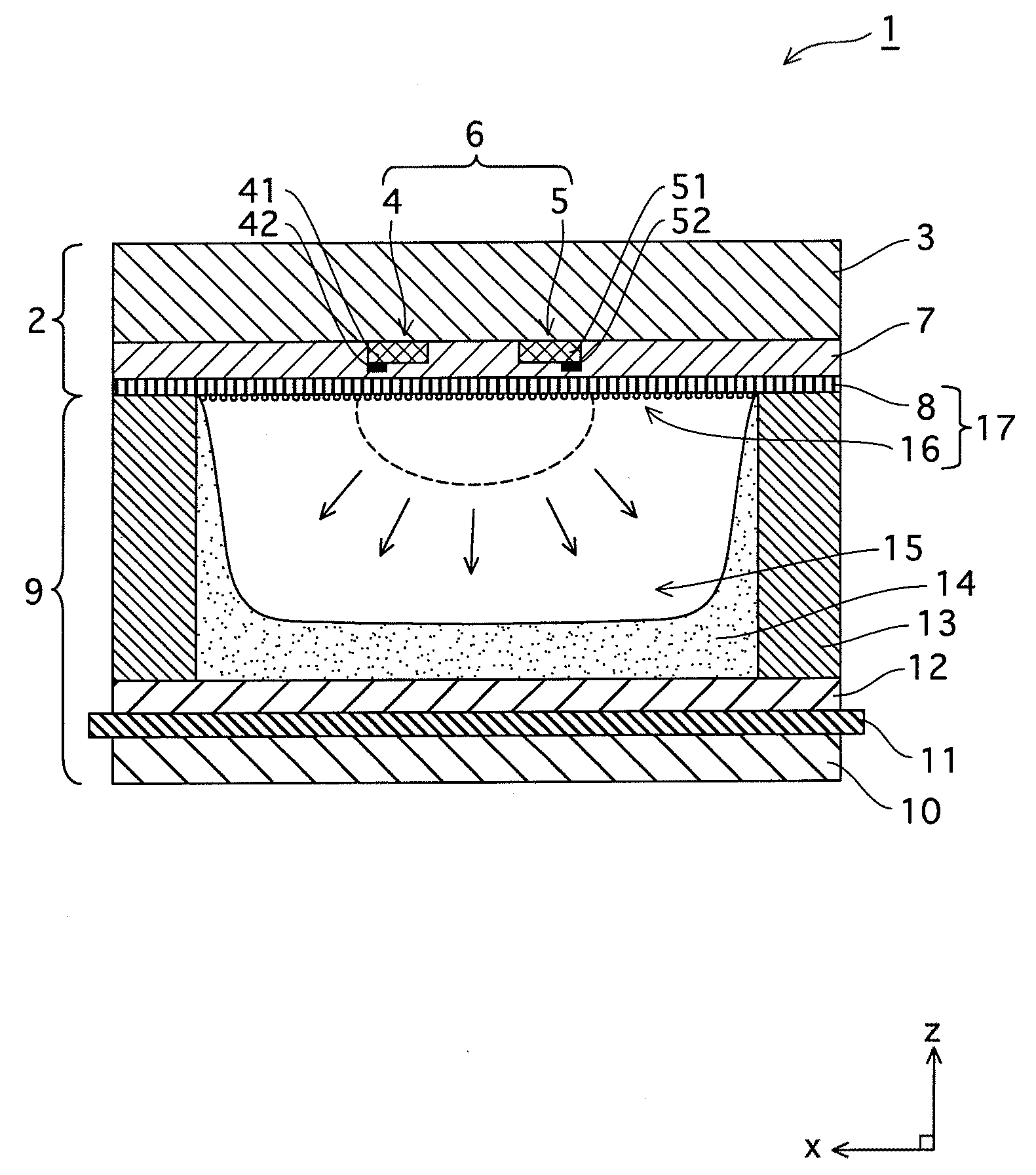
[0063]FIG. 1 is a schematic sectional view of a PDP 1 in accordance with Embodiment 1 of the present invention, the section being taken along the x-z plane. The structure of the PDP 1 is basically identical with that of a conventional PDP (FIG. 10) except for the structure in the vicinity of the protective layer.

[0064]The PDP 1 is an AC PDP with a 42-inch screen in conformity with the NTSC specification. The present invention may be, of course, applied to other specifications such as XGA and SXGA. The applicable specifications of the high-definition PDP that is able to display images at a higher resolution than an HD (high-definition) PDP are PDPs with a size of 37, 42, and 50 inches having 24×720 (pixels), 1024×768 (pixels), and 1366×768 (pixels), respectively. In addition, such a PDP is also applicable to display images at higher resolution than the PDP 1. Examples of a PDP having higher-definition pixels than the HD PDP include a full HD PDP with 1920×1080 (pixels...

embodiment 2

[0128]Following is a description of a PDP 1a in accordance with Embodiment 2 of the present invention. The differences between the PDP 1 and the PDP 1a are mainly described. FIG. 7 is a cross-sectional view of the PDP 1a. FIG. 4B is a schematic view showing the protective layer of the PDP 1a and its nearby portion.

[0129]The feature of the PDP 1a is that the protective layer is composed of the MgO powder 16 disposed directly on the dielectric layer 7 does not include the surface layer 8. The MgO powder 16 includes the MgO particles 16a-16d as with Embodiment 1.

[0130]The PDP 1a with the above feature promotes the smooth secondary electron emission in the wide temperature range from low to a normal temperature or higher when the PDP 1a is initially driven. Thus, the PDP 1a can display excellent images by effectively suppressing the “discharge delay” and “dependence of discharge delay on temperatures.” In addition, the MgO particle 16c included in the MgO powder 16 can improve the depen...

experiment 1

Evaluation of MgO Particle's Crystal Face

[0188]With use of Samples 1, 4, 5, 7-9, a ratio of a surface area of the (100) crystal face to a surface area of the (111) crystal face of each MgO particle of the protective layer was measured. Although the area ratio can be actually measured by visual observation with an electron microscope, the crystal faces are comprehensively identified by an analysis with electron beams and the like in this experiment.


PUM

PropertyMeasurementUnit
particle diameteraaaaaaaaaa
sizeaaaaaaaaaa
sizeaaaaaaaaaa

Abstract

“Discharge delay” and “dependence of discharge delay on temperatures” are solved by improving a protective layer, thus a PDP can be driven at a low voltage. Furthermore, the PDP can display excellent images by suppressing “dependence of discharge delay on space charges.” Liquid-phase magnesium alkoxide (Mg (OR)2) or acetylacetone magnesium ate whose purity is 99.95% or more is prepared, and is hydrolyzed by adding a small amount of acids to the solution. Thus, a gel of magnesium hydroxide that is a magnesium oxide precursor is formed. Burning the gel in atmosphere at 700° C. or more produces powder containing MgO particles 16a-16d having the NaCl crystal structure with (100) and (111) crystal faces or with (100), (110) and (111) crystal faces. By pasting the powder on a dielectric layer 7 or a surface layer 8, the MgO powder 16 is formed so as to serve as the protective layer.

Description

TECHNICAL FIELD[0001]The present invention relates to a plasma display panel and a manufacturing method therefor. The present invention relates more particularly to a plasma display panel having a dielectric layer covered with an improved protective layer, and a method for manufacturing the same.BACKGROUND ART[0002]A plasma display panel (herein after referred to as PDP) is a flat display device that takes advantage of radiation caused by gas discharge. The PDP has been in practical use in many fields such as an image display device and a public information display device, since the PDP can achieve high-speed display and be produced in a large size. There are two types of PDP, a direct-current (DC) type and an alternating-current (AC) type. Especially, the AC surface discharge PDP possesses a high technological potential for realizing a long life and a large-screen display, and therefore has been commercialized.[0003]FIG. 10 is a schematic view showing a structure of a discharge cel...

Claims


Application Information

Patent Timeline
Patent Type & Authority Applications(United States)
IPC IPC(8): H01J17/49H01J11/00C01F5/08C30B29/60H01J9/20H01J9/36H01J11/12H01J11/22H01J11/24H01J11/26H01J11/34H01J11/40H01J11/46
CPCC01F5/02H01J11/40C01F5/08C01F5/12C01P2002/77C01P2002/90C01P2004/03C01P2004/38C01P2004/41C01P2004/52C01P2004/61C01P2004/62C01P2006/80H01J9/02H01J11/12C01F5/06H01J11/38
Inventor FUKUI, YUSUKETERAUCHI, MASAHARUTSUJITA, TAKUJI
Owner PANASONIC CORP
Why Eureka
Try Eureka