Large-scale display device

a display device and large-scale technology, applied in static indicating devices, instruments, non-linear optics, etc., can solve the problems of inability to meet the requirements of panel transmission ratio simultaneously, the active area cannot be enlarged, and the pixel aperture ratio is smaller and smaller, so as to improve the transmission ratio, increase the active area, and increase the resolution of the panel

Inactive Publication Date: 2009-06-04
ADVANCED OPTOELECTRONICS TECH
View PDF1 Cites 8 Cited by
  • Summary
  • Abstract
  • Description
  • Claims
  • Application Information

AI Technical Summary

Benefits of technology

[0009]One aspect of the present invention is to increase the resolution of both the active area of a display device and the margin of the display panel. Furthermore, it achieves both increased panel resolution and improved transmission ratio simultaneously. Therefore, the present invention has the economic advantages for industrial applications.

Problems solved by technology

Even if panel size is increased, array and cell processes cannot assemble mass panels.
Although panel resolution can be increased, panel transmission ratio requirements cannot be met simultaneously.
A challenge in the TFT-LCD industry is the pursuit of increasingly large panel sizes, as well as higher resolution, resulting in smaller and smaller pixel aperture ratios.
Even if the aperture ratio of each pixel is increased by enlarging panel size, gain is limited.
Both panel resolution and light transmission cannot be increased simultaneously.

Method used


Image

  • Large-scale display device
  • Large-scale display device
  • Large-scale display device

Examples


Embodiment Construction

[0016]The present invention describes a large-scale display device. Detailed descriptions of the structure and elements are provided in order to make the invention thoroughly understood. Obviously, the application of the invention is not limited to specific details provided herein; the common structures and elements that are known to those who are skilled in the art are not described in detail to avoid unnecessary limitations of the invention.

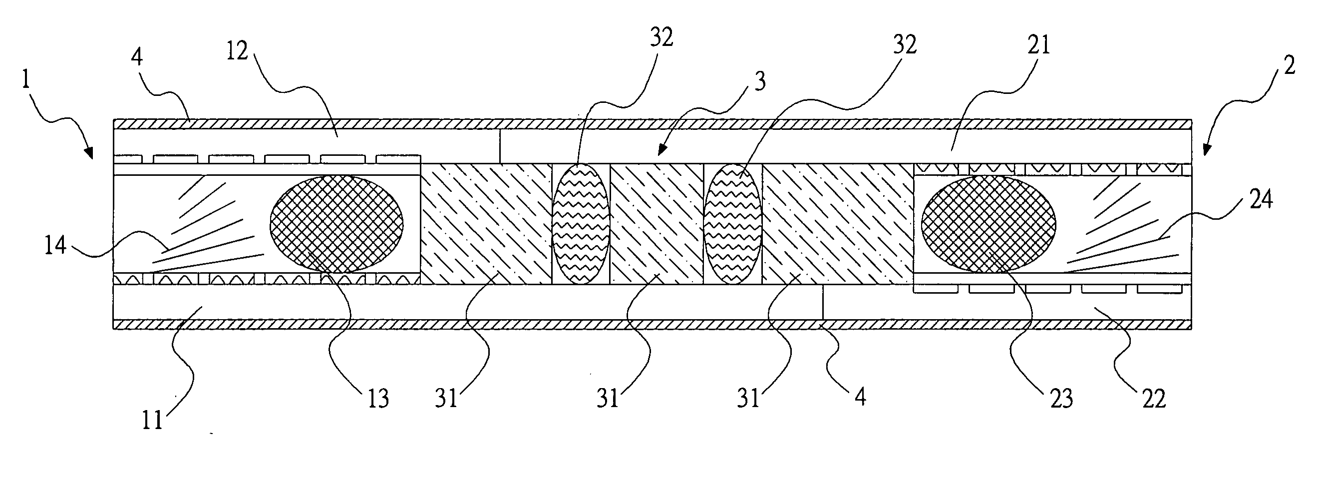
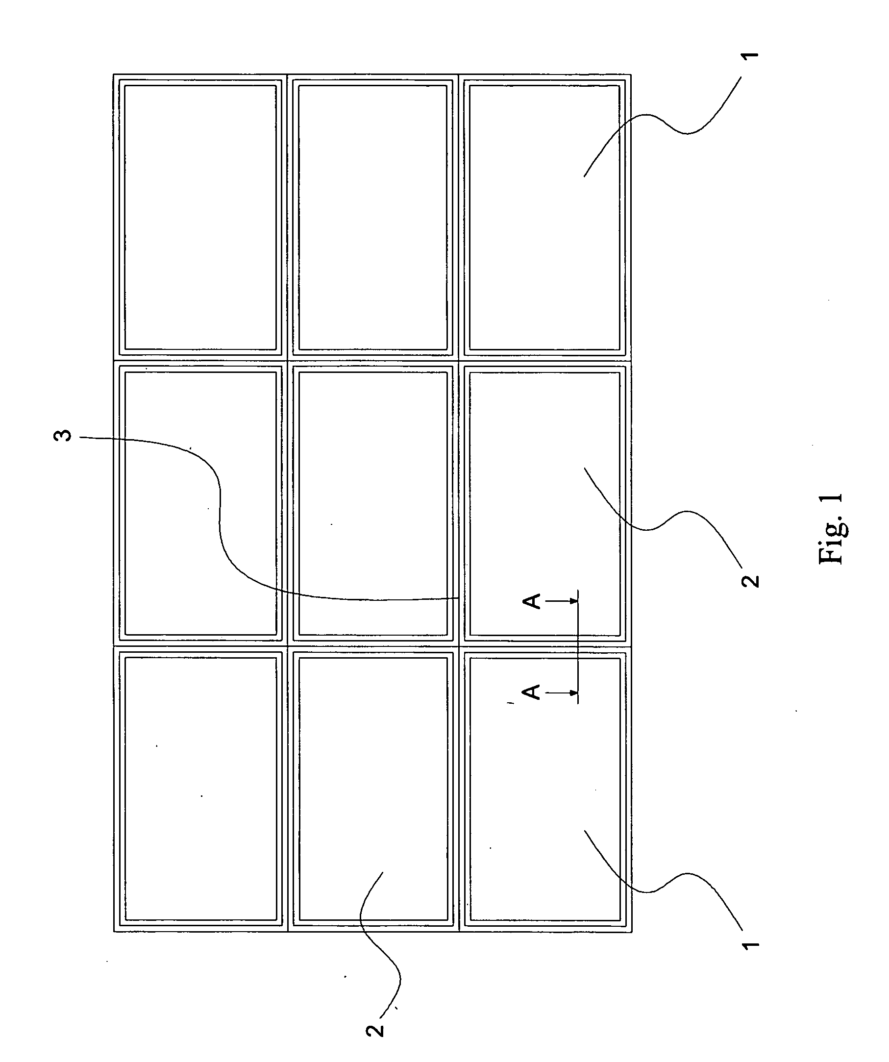
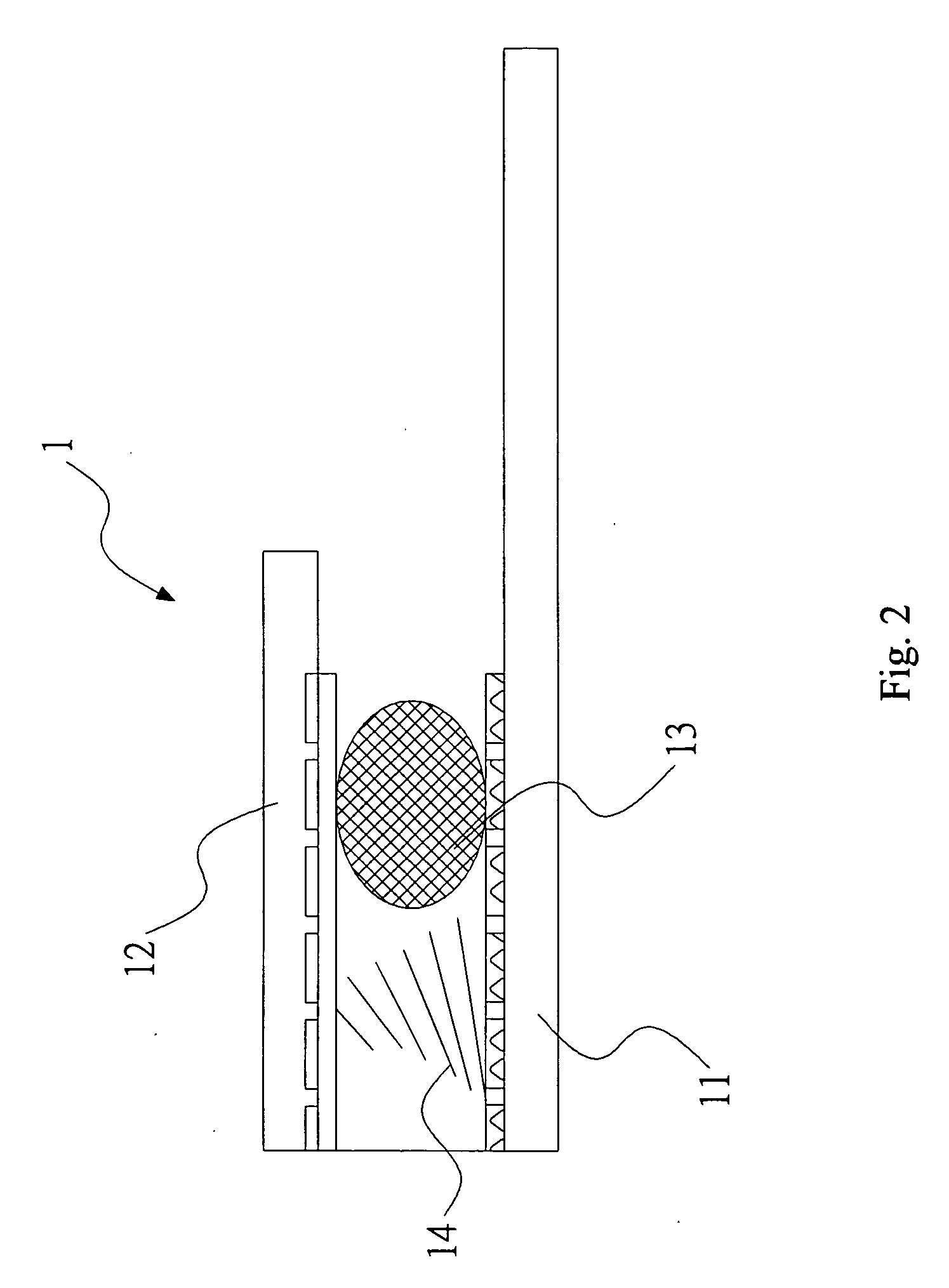
[0017]Please refer to FIG. 1, FIG. 2, FIG. 3 and FIG. 4, in which the present invention is illustrated by schematic diagrams of a top view, a sectional view to the first display unit, a sectional view to the second display unit, and a cross-sectional view along the A-A line of FIG. 1. This invention provides a large-scale display device including at least a first display unit 1, at least a second display unit 2, black margin areas 3, and polarizer4.

[0018]The first display unit 1 comprises a first thin film transistor substrate 11 (TFT substrate...


PUM

PropertyMeasurementUnit
lengthaaaaaaaaaa
lengthaaaaaaaaaa
sizeaaaaaaaaaa

Abstract

The present invention discloses a large-scale display device, which comprises a first display unit, a second display unit, a black margin area between the first display unit and the second display unit, and two polarizers attached to two surfaces of the first and second display units. The second display unit is arranged in parallel to the first display unit.

Description

BACKGROUND OF THE INVENTION[0001](A) Field of the Invention[0002]The present invention is generally related to a large-scale display device, and more particularly to a display device featuring increased active area size, better resolution at the display panel margins, and increased pixel aperture ratio to provide higher resolution and better light transmission ratio.[0003](B) Description of the Related Art[0004]A traditional TFT-LCD panel is fabricated by means of a forepart array process to form thin film transistors on a glass (TFT substrate), and an intermediate cell process to fasten and seal the TFT substrate to another glass with color filter thereon (CF substrate). Liquid crystal is then injected into the space between the TFT substrate and CF substrate to form an active area, wherein each pixel includes red (R), green (G), and blue (B) colors. When electric current flows through the transistors to generate electric field variations to cause rotation of liquid crystal molecul...

Claims


Application Information

Patent Timeline
Patent Type & Authority Applications(United States)
IPC IPC(8): G02F1/133
CPCG02F1/13336G02F1/1339G02F1/133528
Inventor CHIU, KUAN HER
Owner ADVANCED OPTOELECTRONICS TECH
Why Eureka
Try Eureka