Dual gate oxide structure in semiconductor device and method thereof

a technology of oxide structure and semiconductor, applied in the manufacturing of semiconductor/solid-state devices, basic electric elements, electric devices, etc., can solve the problems of relative the active region to have a fixed size, and the severe dent on the boundary face between the active region and the field region. to achieve the effect of preventing a dent and enhancing a device characteristi

Inactive Publication Date: 2007-07-31
SAMSUNG ELECTRONICS CO LTD
View PDF8 Cites 10 Cited by
  • Summary
  • Abstract
  • Description
  • Claims
  • Application Information

AI Technical Summary

Benefits of technology

[0019]Example embodiments of the present invention provide a dual gate oxide structure in a semiconductor device and a method of forming the structure, which is capable of extending an area of active region by utilizing a trench sidewall portion of the device isolation layer as the active region. Herewith, a cell current of the active region can increase to enhance a characteristic of the device. In addition, a stringer caused by a stepped coverage between an active region and a field region can be prevented, and it can prevent a dent caused on a boundary face between the active region and the field region owing to a wet etching rate difference between field oxide material formed on a STI and thermal oxide material formed on the active region.

Problems solved by technology

However, in applying a dual gate oxide to the STI structure using manufacturing processes of the prior art, an uppermost part of the device isolation layer is positioned higher than an upper surface of active region, which causes a stepped coverage therebetween.
This also causes a relatively severe dent on a boundary face between the active region and the field region owing to a wet etching rate difference between materials of a field oxide layer formed in the STI and a thermal oxide layer formed in the active region.
Even though this structure of dual gate oxide layer based on the prior art can increase an integration of device, a size of active region has a fixed structure, and an upper part of STI is positioned higher than an upper part of the active region, causing a stepped structure, thus there are many problems as follows.
First, since the upper part of STI is positioned higher than an upper part of the active region, i.e., the stepped structure, a trench sidewall portion can not be used as the active region, which causes the active region to have a fixed size.
Further, the STI is formed of field oxide material such as USG or HDP etc., and the gate oxide layer is formed of thermal oxide material, thus in using an etching process to form the dual gate oxide layer, a severe dent is caused on a boundary face between the active region and the field region owing to a wet etching rate difference between the field oxide layer and the thermal oxide layer.

Method used


Image

  • Dual gate oxide structure in semiconductor device and method thereof
  • Dual gate oxide structure in semiconductor device and method thereof
  • Dual gate oxide structure in semiconductor device and method thereof

Examples


Embodiment Construction

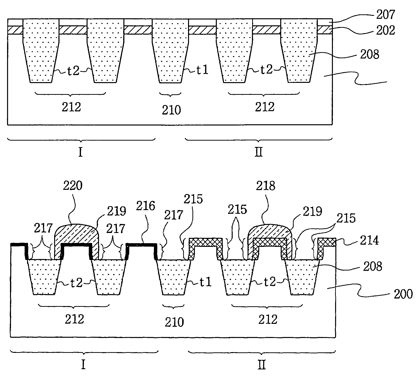
[0025]The present invention and example embodiments, thereof, are more fully described below with reference to FIGS. 2a through 2h. This present invention may, however, be embodied in many different forms and should not be construed as being limited to the example embodiments set forth herein. Rather, these example embodiments are provided so that this disclosure is thorough and complete, and conveys the concept of the present invention to those skilled in the art.

[0026]FIGS. 2a to 2h are diagrams illustrating a sequential process of dual gate oxide forming method according to an exemplary embodiment of the present invention. The process classified into eight steps for convenience will be described as follows.

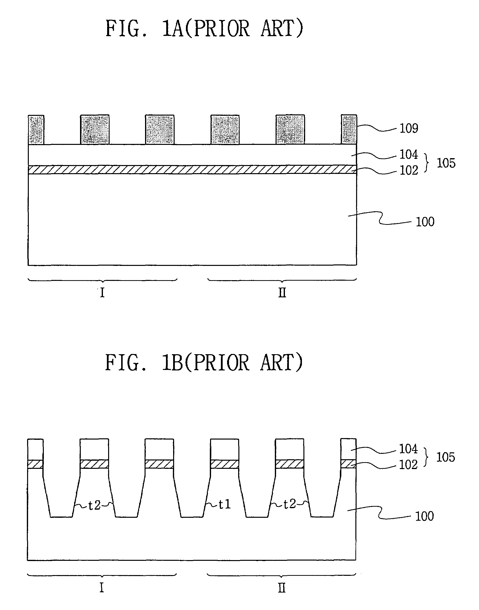
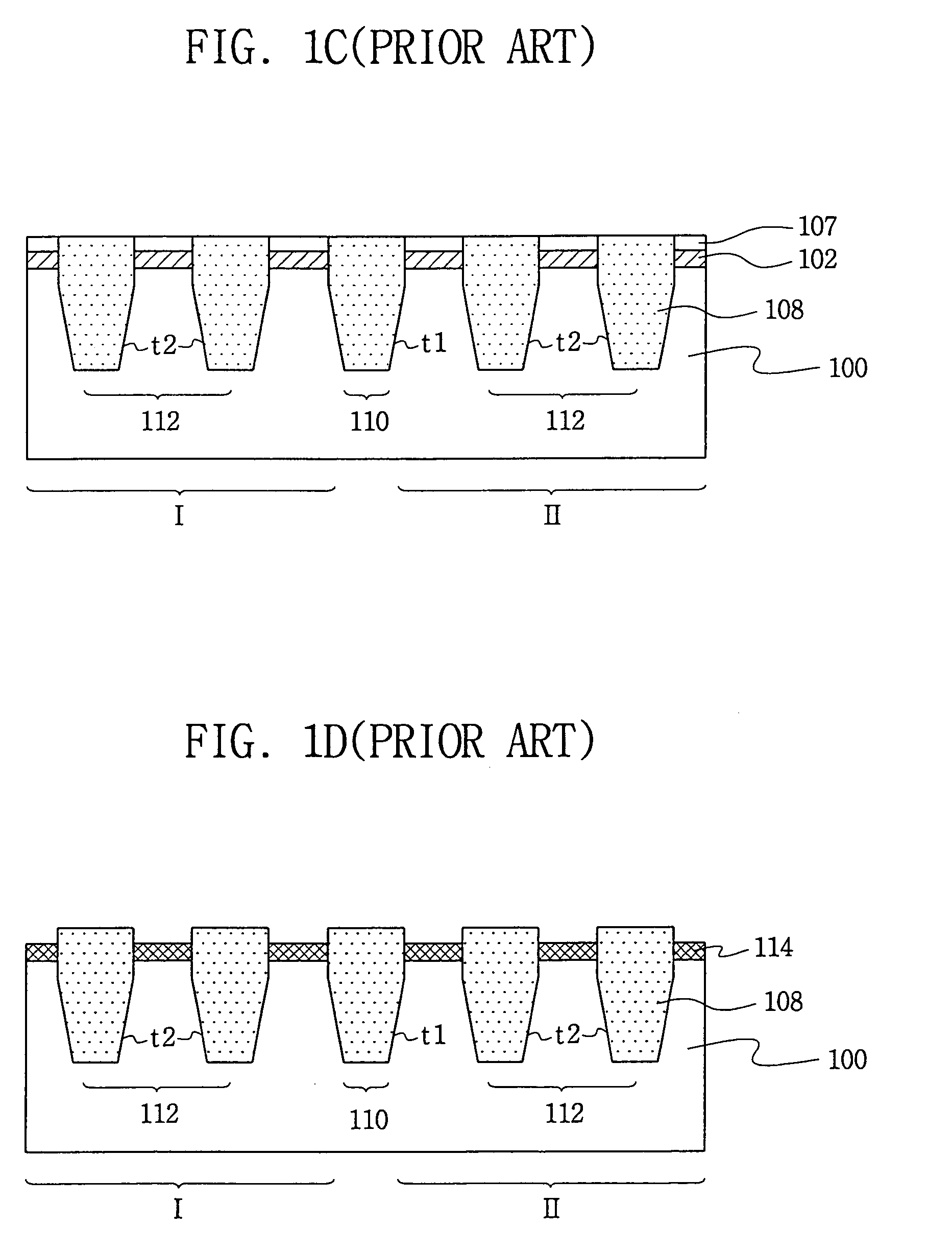
[0027]Reference character I indicates a low voltage (LV) region as a first active region on which a thinned gate oxide layer will be formed, and reference character II designates a high voltage (HV) region as a second active region on which a thick gate oxide layer will be form...


PUM


Abstract

In the method of manufacturing a dual gate oxide layer of a semiconductor device, which has first and second active regions operating at mutually different voltages on a semiconductor substrate, the first and second active regions having a device isolation layer of STI (Shallow Trench Isolation) structure; the method of manufacturing the dual gate insulation layer includes, forming the device isolation layer so that an uppermost part thereof is positioned lower than an upper surface of the first and second active regions, before forming a gate insulation layer corresponding to each of the first and second active regions. Whereby, it is be effective till a portion of trench sidewall utilized as the active region, to increase a cell current of the active region and to prevent a stringer caused by a stepped coverage between the active region and a field region and a dent caused on a boundary face between the active region and the field region.

Description

CROSS-REFERENCE TO RELATED APPLICATIONS[0001]This application claims priority from Korean Patent Application 2003-0040714, filed Jun. 23, 2003, the contents of which are incorporated herein by reference.FIELD OF THE INVENTION[0002]This disclosure relates to a semiconductor device, and more particularly, to a method of forming a dual gate oxide having oxide layers based on different thickness in different voltage regions.PRIOR ART OF THE INVENTION[0003]In a semiconductor memory device such as an SRAM etc., an operating voltage of a transistor constituting a memory cell and an operating voltage of transistor positioned within a peripheral logic circuit to access data of the memory cell are typically different from each other, thus a thickness of gate insulation layers, e.g., oxide layers, are also different. Further, in the field of power devices such as LDI (LCD Driver IC) products, a low voltage operation for driving a logic circuit and a high voltage operation for driving an LCD ar...

Claims


Application Information

Patent Timeline
Patent Type & Authority Patents(United States)
IPC IPC(8): H01L21/336H01L21/762H01L21/8234
CPCH01L21/76229H01L21/823462H01L21/823481H01L21/18
Inventor CHUN, JONG-SIKJO, HYUN-HOCHUNG, BYUNG-HONG
Owner SAMSUNG ELECTRONICS CO LTD
Why Eureka
Try Eureka