Method for manufacturing soi substrate

a technology of soi substrate and substrate, which is applied in the direction of semiconductor devices, basic electric elements, electrical apparatus, etc., can solve the problems of increasing the adhesion defect factor, increasing the possibility of adhesion defects, and voids, so as to achieve high bonding strength, reduce adhesion defects between a single crystal semiconductor layer and a support substrate, and high bonding strength

Inactive Publication Date: 2009-06-04
SEMICON ENERGY LAB CO LTD
View PDF58 Cites 324 Cited by
  • Summary
  • Abstract
  • Description
  • Claims
  • Application Information

AI Technical Summary

Benefits of technology

[0017]When the present invention is applied, adhesion defects between a single crystal semiconductor layer and a support substrate are reduced, and an SOI

Problems solved by technology

However, in a step of bonding a silicon wafer and a glass substrate, when minute foreign matter (dust, an abrasive remaining on the surface of the glass substrate, or the like) is attached to the adhesion interface between the silicon wafer and the glass substrate, an abundance of voids occur, which becomes a factor of increase in adhesion defects.
Further, if bubbles are taken into part of the adhesion interface due to warpage or deflection of the glass substrate, the possibility of occurrence of adhesion defects is increased.
Still furth

Method used


Image

  • Method for manufacturing soi substrate
  • Method for manufacturing soi substrate
  • Method for manufacturing soi substrate

Examples


embodiment mode 1

[0052]In this embodiment mode, a method for manufacturing an SOI substrate, in which a single crystal semiconductor substrate is divided into a single crystal semiconductor layer bonded to a support substrate and a single crystal semiconductor substrate, and a surface of the single crystal semiconductor layer bonded to the support substrate is pressed, will be described with reference to the drawings. Further, in this embodiment mode, a method for manufacturing an SOI substrate, which is aimed at providing a single crystal semiconductor layer over a substrate having low heat-resistant temperature, such as a glass substrate will also be described.

[0053]First, a single crystal semiconductor substrate 101 is prepared. The single crystal semiconductor substrate 101 is processed to have a desired size and shape. The single crystal semiconductor substrate 101 is, for example, a single crystal silicon substrate, a germanium substrate, a semiconductor substrate made of a compound such as ga...

embodiment mode 2

[0167]In this embodiment mode, a method for manufacturing an SOI substrate, which is different from that shown in Embodiment Mode 1 will be described with reference to FIGS. 12A to 12C. Hereinafter, the portions similar to those in Embodiment Mode 1 are denoted by the same reference numerals, and description thereof is omitted.

[0168]First, a substrate in which the single crystal semiconductor layer 108 is bonded to the support substrate 107 shown in FIG. 6A with an insulating layer therebetween is prepared, and a mask 118 for selectively removing the single crystal semiconductor layer 108 is formed over the single crystal semiconductor layer 108 (see FIG. 12A). Note that the mask 118 can be formed using a photolithography process or ink-jet printing. Here, the mask may have any shape, area, or the like; however, it is formed so that the single crystal semiconductor layer 108 can be processed into a desired shape, area, or the like.

[0169]Next, the single crystal semiconductor layer 1...

embodiment mode 3

[0174]In this embodiment mode, a method for manufacturing an SOI substrate, which is different from that shown in the above embodiment mode will be described with reference to FIGS. 13A to 13C and FIGS. 14A to 14C. Hereinafter, the portions similar to those in Embodiment Mode 1 are denoted by the same reference numerals, and description thereof is omitted.

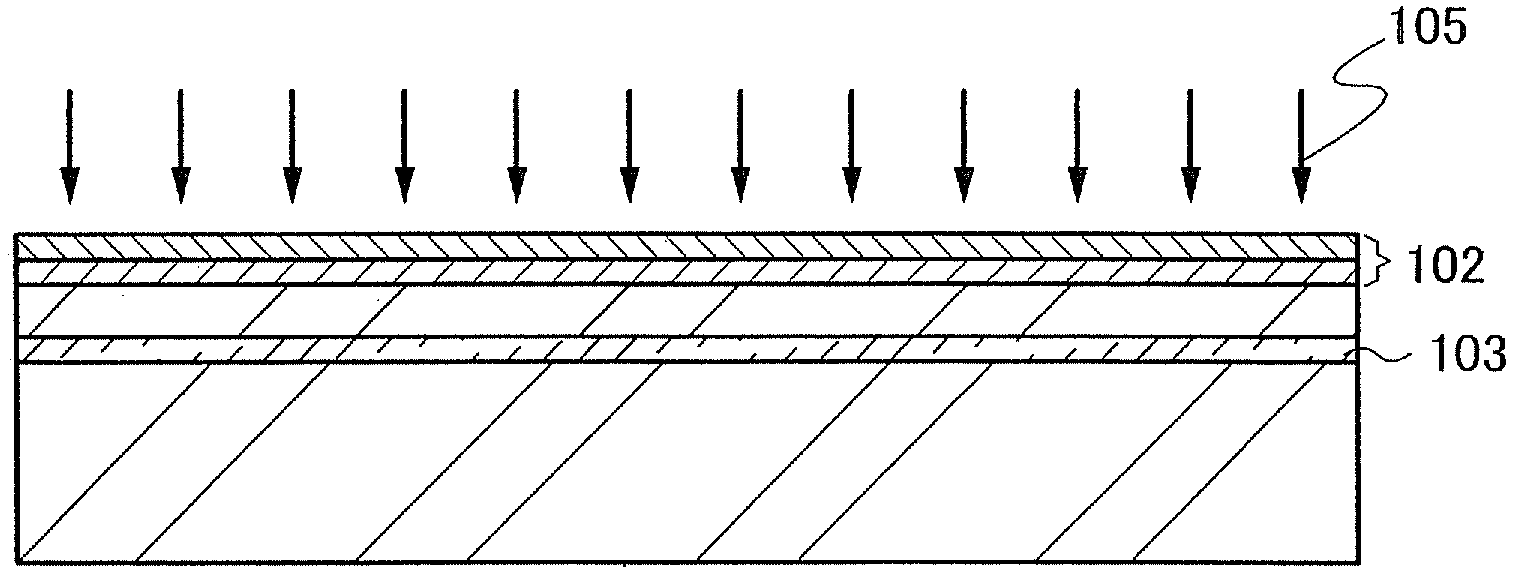
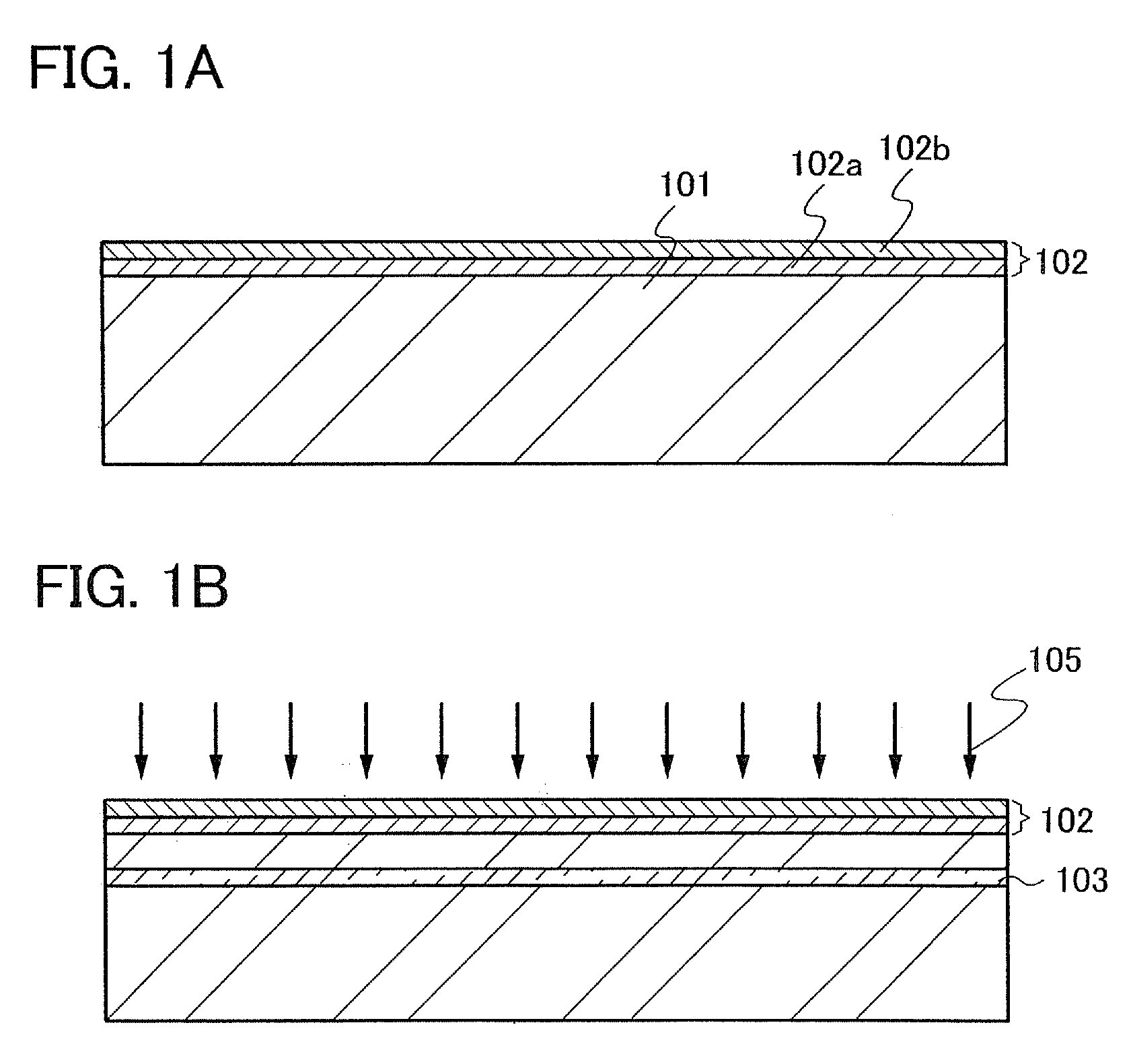
[0175]As shown in FIG. 13A, the insulating layer 102 including a silicon oxynitride layer 102a and a silicon nitride oxide layer 102b is formed over the single crystal semiconductor substrate 101. Next, as shown in FIG. 13B, through the insulating layer 102, the single crystal semiconductor substrate 101 is irradiated with an ion beam 105 including ions accelerated by an electric field, so that the ions are introduced into the single crystal semiconductor substrate 101; accordingly, a damage region 103 is formed in a region at a predetermined depth from one of surfaces of the single crystal semiconductor substrate 101. Then, as sho...


PUM


Abstract

Adhesion defects between a single crystal semiconductor layer and a support substrate are reduced to manufacture an SOI substrate achiving high bonding strength between the single crystal semiconductor layer and the support substrate. Plasma is produced by exciting a source gas, ion species contained in the plasma are added from one surface of a single crystal semiconductor substrate, and thereby forming a damage region in the single crystal semiconductor substrate; forming an insulating layer over one surface of the single crystal semiconductor substrate; a support substrate is bonded so as to face the single crystal semiconductor substrate with the insulating layer therebetween; the single crystal semiconductor substrate is heated to separate the single crystal semiconductor substrate into a single crystal semiconductor layer bonded to the support substrate and a single crystal semiconductor substrate, in the damage region; and the single crystal semiconductor layer bonded to the support substrate is pressed.

Description

BACKGROUND OF THE INVENTION[0001]1. Field of the Invention[0002]The present invention relates to a method for manufacturing an SOI substrate having a semiconductor layer on its insulating surface.[0003]2. Description of the Related Art[0004]In recent years, a technique for forming a thin film transistor (TFT) using a semiconductor thin film (a thickness of approximately several nanometers to several hundred nanometers) formed over a substrate having an insulating surface of glass or the like has attracted attention. Thin film transistors are applied to a wide range of electronic devices such as integrated circuits and electro-optic devices, and rapid development of thin film transistors that are to be used as switching elements in image display devices, in particular, has been pushed.[0005]Instead of silicon wafers that are manufactured by thinly slicing an ingot of a single crystal semiconductor, semiconductor substrates called silicon on insulator (SOI) substrates have been develo...

Claims


Application Information

Patent Timeline
IPC IPC(8): H01L21/30
CPCH01L21/76254Y10S438/977Y10S438/928
Inventor YAMAZAKI, SHUNPEI
Owner SEMICON ENERGY LAB CO LTD
Why Eureka
Try Eureka