Semiconductor device and manufacturing method thereof, and camera module including the same

a technology of semiconductor devices and manufacturing methods, applied in semiconductor devices, semiconductor/solid-state device details, electrical apparatus, etc., can solve problems such as optical devices, defective packaging of camera modules and the like, and increase the time of sealing resin drop, so as to prevent the effect of running, the manufacturing yield of semiconductor devices can be improved, and the drop of sealing resin is not increased

Active Publication Date: 2009-06-11
PANASONIC SEMICON SOLUTIONS CO LTD
View PDF7 Cites 8 Cited by
  • Summary
  • Abstract
  • Description
  • Claims
  • Application Information

AI Technical Summary

Benefits of technology

[0032]In the method for manufacturing a semiconductor device according to the invention, the sealing resin can be prevented from running onto a top surface of the frame even when ripples are generated at a surface of the sealing resin when the dropping nozzle is lifted to finish filling of the sealing resin. This is because the groove is formed on an upper end of the frame on the semiconductor element side (inner side) of the frame by removing at least the upper corner portion of the frame and the groove thus formed can accept the sealing resin. As a result, manufacturing yield of the semiconductor device can be improved. Moreover, unlike the case where a thinner dropping nozzle is used, the dropping time of the seal

Problems solved by technology

Such overflow of the sealing resin 10 onto the mounting reference surface 13 and the like therefore cause defective packaging of a camera module and the like.
This problem becomes more significant as the optical device (and the frame 2) become

Method used


Image

  • Semiconductor device and manufacturing method thereof, and camera module including the same
  • Semiconductor device and manufacturing method thereof, and camera module including the same
  • Semiconductor device and manufacturing method thereof, and camera module including the same

Examples


Embodiment Construction

[0039]Hereinafter, a semiconductor device according to an embodiment of the invention will be described with reference to the accompanying drawings. An optical device will be herein explained as an example of the semiconductor device.

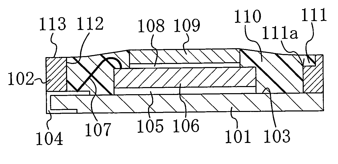
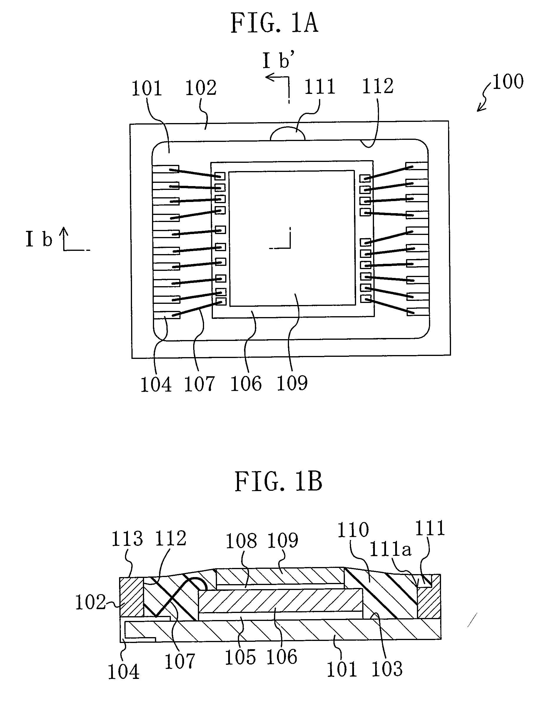
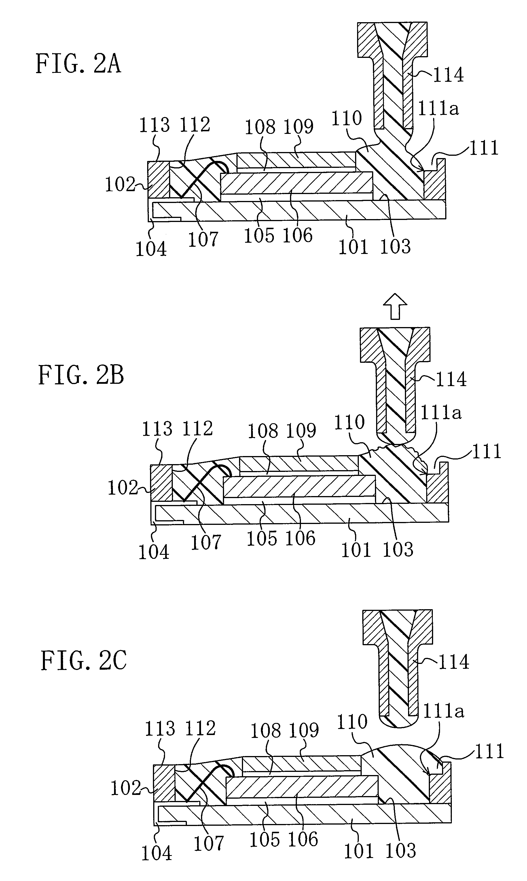
[0040]FIGS. 1A and 1B are diagrams showing a structure of an optical device 100 according to this embodiment. FIG. 1A is a plan view of the optical device 100, and FIG. 1B is a cross-sectional view taken along line Ib-Ib′ in FIG. 1A.

[0041]The optical device 100 is formed by using an insulating base 101 made of a ceramic, a resin, or the like. A frame 102 is provided on the periphery of the insulating base 101, and a surface of the insulating base 101 in a region located inside the frame 102 serves as an element mounting surface 103. A plurality of wiring portions 104 made of, for example, metalized wiring bodies are extended from the periphery of the element mounting surface 103 to a bottom surface of the insulating base 101. An optical function element...


PUM


Abstract

A semiconductor device includes: an insulating base; a semiconductor element provided on the insulating base; a protector provided on the semiconductor element; and a frame provided on a periphery of the insulating base and surrounding the semiconductor element. A region inside the frame is filled with a sealing resin, and at least one groove is provided in an upper corner portion of the frame on the semiconductor element side of the frame.

Description

CROSS REFERENCE TO RELATED APPLICATION[0001]This application claims priority under 35 U.S.C. §119 on Patent Application No. 2007-317305 filed in Japan on Dec. 7, 2007, the entire contents of which are hereby incorporated by reference.BACKGROUND OF THE INVENTION[0002]1. Field of the Invention[0003]The invention relates to a semiconductor device having a semiconductor element mounted on an insulating base, such as an optical device like a solid-state imaging device using an imaging element such as a CCD (Charge Coupled Device) and a CMOS (Complementary Metal-Oxide Semiconductor), and a manufacturing method of the semiconductor device.[0004]2. Related Art[0005]With reduction in size of electronic equipments such as portable terminals, reduction in size of semiconductor devices has been demanded in recent years. In addition to reduction in size and thickness of semiconductor devices, quality of a reference surface is also important for secondary mounting of a semiconductor device onto a...

Claims


Application Information

Patent Timeline
IPC IPC(8): H01L33/00H01L31/0203H01L21/50H01L23/28H01L27/14
CPCH01L23/24H01L31/0203H01L2224/32225H01L2224/49171H01L2224/48227H01L2224/73265H01L2224/45144H01L2224/48091H01L2924/00014H01L2924/00
Inventor TANAKA, SHOICHIOHSAKI, HIROTO
Owner PANASONIC SEMICON SOLUTIONS CO LTD
Why Eureka
Try Eureka